
Chapter 2 Diode Circuits
In the last chapter, we discussed some of the properties of semiconductor materials, and introduced the diode. We presented the ideal current voltage relationship, and considered the piecewise linear model, which simplifies the de analysis of diode circuits. In this chapter, the techniques and concepts developed in Chapter 1 are used to analyze and design electronic circuits containing diodes.
Diode circuits to be considered perform functions such as rectification, clipping. and clamping. These functions are possible only because of the nonlinear properties of the pn junction diode. The conversion of an ac voltage to a dc voltage, such as for a dc power supply, is called rectification. Clipper diode circuits clip portions of a signal that are above or below some reference level. Clamper circuits shift the entire signal by some dc value, Zener diodes, which operate in the reverse-bias breakdown region, have the advantage that the voltage across the diode in this region is nearly constant over a wide range of currents. Such diodes are used in voltage reference or voltage regulator circuits.
Finally, we look at the circuits of two special diodes: the light-emitting diode (LED) and the photodiode. An LED circuit is used in visual displays, such as the seven-segment numerical display. The photodiode circuit is used to detect the presence or absence of light and convert this information into an electrical signal.
Although diodes are useful electronic devices, we will begin to see the limitations of these devices and the desirability of having some type of "amplifying" device.
2.1 RECTIFIER CIRCUITS
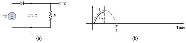
One important application of diodes is in the design of rectifier circuits. A diode rectifier forms the first stage of a dc power supply as shown in Figure 2.1 below.
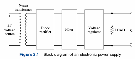
As we will see throughout the text, a dc power supply is required to bias all electronic circuits. The dc output voltage vo will usually be in the range of 3 to 24V depending on the application.
Rectification is the process of converting an ac voltage to one polarity. The diode is useful for this function because of its nonlinear characteristics, that is, current exists for one voltage polarity, but is essentially zero for the opposite polarity. Rectification is classified as half-wave or full-wave, with half-wave being the simplest.
2.1.1 Half-Wave Rectification
Figure 2.2(a) shows a power transformer with a diode and resistor connected to the secondary of the transformer.
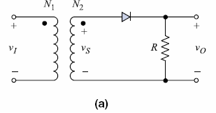
We will use the piecewise linear approach in analyzing this circuit, assuming the diode forward resistance is rf = 0 when the diode is "on."
The input signal vI is often a 120V{rms), 60 Hz ac signal. Recall that the secondary voltage vs and primary voltage, vI of an ideal transformer are related by
![]()
where N1 and N2 are the number of primary and secondary turns, respectively. This ratio is called the transformer turns ratio.
Note when using the piecewise linear model of the diode, we typically determine the linear regions (conducting or not) in which the diode is operating by
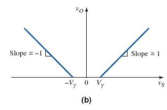
Figure 2.2(b) shows the voltage transfer characteristics. v0 versus vs, for the circuit.
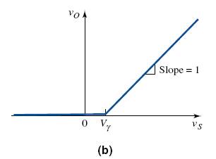
When vs < 0, the diode is reverse biased, which means that the current is zero and the output voltage is zero. As long as vs < Vγ , the diode will be non-conducting, so the output voltage will remain zero. When
vs > Vγ, the diode becomes forward biased and a current is induced in the circuit. In this case, we can write
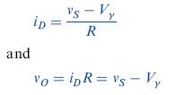
For vs > Vγ, the slope of the transfer curve is 1.
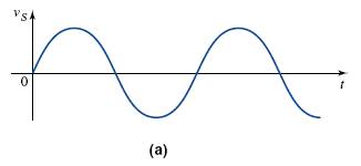
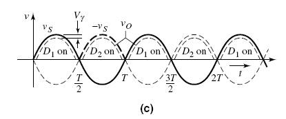
If vs is a sinusoidal signal, as shown in Figure 2.3(a),
the output voltage can be found using the voltage transfer curve in Figure 2.2(b) above.
and is shown in the figure below.
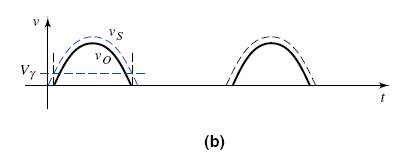
We can see that while the input signal vs alternates polarity and has a time-average value of zero, the output voltage vo is unidirectional and has an non-zero average value, and is therefore rectified. Since the output voltage appears only during the positive cycle of the input signal, the circuit is called a half-wave rectifier.
When the diode is cut off and non-conducting, no voltage drop occurs across the resistor R: therefore, the entire input signal voltage appears across the diode as shown below.
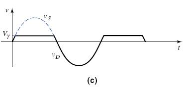
Consequently, the diode must be capable of handling the peak current in the forward direction and sustaining a large peak inverse voltage (PIV) without breakdown.
One disadvantage of the half-wave rectifier is that we "waste" the negative half-cycles. The current is zero during the negative half-cycles, so there is no energy dissipated, but at the same time, we are not making use of any possible available energy.
2.1.2 Full-Wave Rectification
A full-wave rectifier inverts the negative portions of the sine wave so that a unipolar output signal is generated during both halves of the input sinusoid. One example of a full-wave rectifier circuit appears in Figure 2.6(a).
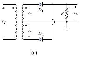
The input to the rectifier consists of a power transformer, in which the input is normally a 120V (rms), 60Hz ac signal, and the two outputs are from a center-tapped secondary winding that provides equal voltages vs, with the polarities shown. When the input line voltage is positive, both output signal voltages vs are also positive. The input power transformer also provides electrical isolation between the power-line circuit and the electronic circuits to be biased by the rectifier circuit. This isolation reduces the risk of electrical shock.
During the positive half of the input voltage cycle, both output voltages vs are positive; therefore, diode D1 is forward biased and conducting and D2 is reverse biased and cut-off. The current through D1 and the output resistance produce a positive output voltage. During the negative half cycle the situation with the diodes is reversed. If we assume that the forward diode resistance rf of each diode is negligible, we obtain the voltage transfer characteristics, yo versus vS shown in Figure 2.6(b).
For a sinusoidal input voltage, we can determine the output voltage versus time by using the voltage transfer curve shown in Figure 2.6(b). The corresponding input and output voltage signals are shown in Figure 2.6(c).
Since a rectified output voltage occurs during both the positive and negative cycles of the input signal, this circuit is called a full-wave rectifier.
Another example of a full-wave rectifier circuit appears in Figure 2.7(a).
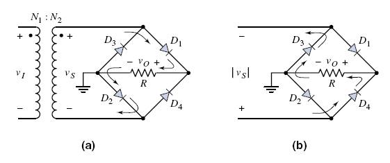
This circuit is a bridge rectifier, which provides electrical isolation between the input ac power-line and the rectifier output, but does not require a center-tapped secondary winding. However, it does use four diodes.
During the positive half of the input voltage cycle, vs is positive, Dl and D2 are forward biased. D3 and D4 are reverse biased, and the direction of the current is as shown in Figure 2.7(a). During the negative half-cycle of the input voltage, vs is negative, and D3 and D4 are forward biased. The direction of the current, shown in Figure 2.7(b), produces the same output voltage polarity as before.
Figure 2.7{c) shows the sinusoidal voltage vs and the rectified output voltage vo.
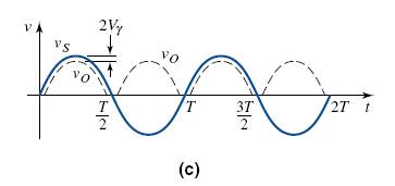
Because two diodes are in series in each of the conduction paths, the magnitude of v0 is two diode drops less than the magnitude of vs.
2.1.3 Filters, Ripple Voltage, and Diode Current
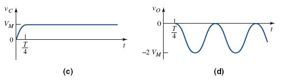
If a capacitor is added in parallel with the load resistor of a half-wave rectifier to form a simple filter circuit (Figure 2.8(a)), we can begin to transform the half-wave sinusoidal output into a dc voltage. Figure 2.8(b) shows the positive half of the output sine wave, and the beginning portion of the voltage across the capacitor, assuming the capacitor is initially uncharged.
When the signal voltage reaches its peak and begins to decrease, the voltage across the capacitor also starts to decrease, which means the capacitor starts to discharge. The only discharge current path is through the resistor. If the RC time constant is large, the voltage across the capacitor discharges exponentially with time (Figure 2.8(c)). During this time period, the diode is cut-off.
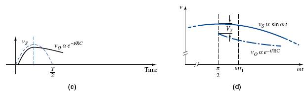
A more detailed analysis of the circuit response when the input voltage is near its peak value indicates a subtle difference between actual circuit operation and the qualitative description. If we assume that the diode turns off immediately when the input voltage starts to decrease from its peak value, then the output voltage will decrease exponentially with time, as previously indicated. An exaggerated sketch of these two voltages is shown in Figure 2.8(d). The output voltage decreases at a faster rate than the input voltage,
which means that at time t1 the voltage across the diode, is greater than Vγ. However, this condition cannot exist and the diode does not turn off immediately. If the RC time constant is large, there is only a small difference between the time of the peak input voltage and the time the diode turns off.
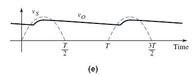
During the next positive cycle of the input voltage, there is a point at which the input voltage is greater than the capacitor voltage, and the diode turns back on. The diode remains on until the input reaches its peak value and the capacitor voltage is completely recharged.
Since the capacitor filters out a large portion of the sinusoidal signal, it is called a filter capacitor. The steady-state output voltage of the RC filter is shown in Figure 2.8(e).
The ripple effect in the output from a full-wave filtered rectifier circuit can be seen in the output waveform in Figure 2.9.
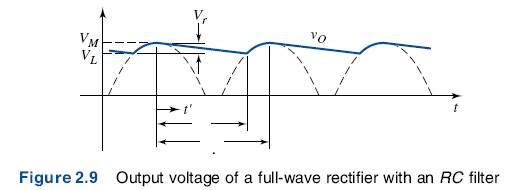
The capacitor charges to its peak voltage value when the input signal is at its peak value. As the input decreases, the diode becomes reverse biased and the capacitor discharges through the output resistance R. Determining the ripple voltage is necessary for the design of a circuit with an acceptable amount of ripple. The derivation of this is on p. 58 of your text.
If we can assume that the ripple effect is small we get the following approximation
![]()
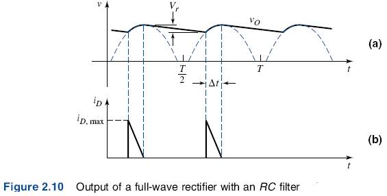
where Tp is the time between peak values of the output voltage.
For a full-wave rectifier Tp is one-half the signal period. Therefore, we can relate Tp to the signal frequency,

and the ripple voltage becomes
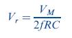
The diode in a filtered rectifier circuit conducts for a brief interval Δt near the peak of the sinusoidal input signal (Figure 2.10{a)).
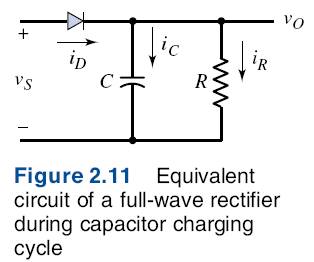
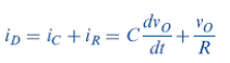
The diode current supplies the charge lost by the capacitor during the discharge time. Figure 2.11 shows the equivalent circuit of the full-wave rectifier during the charging time.
We see that
The text derives an approximation for the average and maximum diode current on p. 60.
2.1.4 Voltage Doubler Circuit
A voltage doubter circuit is very similar to the full-wave rectifier, except that two diodes are replaced by capacitors, and it can produce a voltage equal to approximately twice the peak output of a transformer (Figure 2.13).
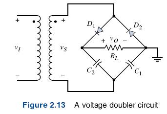
Figure 2.14(a) shows the equivalent circuit when the voltage polarity at the ""top" of the transformer is negative; Figure 2.14(b) shows the equivalent circuit for the opposite polarity. In the circuit in Figure 2.14(a), the forward diode resistance of D2 is small; therefore, the capacitor C, will charge to almost the peak value of vs. Terminal 2 on C1 is positive with respect to terminal 1. As the magnitude of vs decreases from its peak value, C1 discharges through RL and C2. We assume that the time constant RLC2 is very long compared to the period of the input signal.
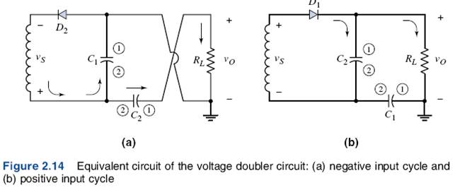
As the polarity of vs changes to that shown in Figure 2.14(b), the voltage across C1, is essentially constant at VM , with terminal 2 remaining positive. As vs reaches its maximum value, the voltage across C2 essentially becomes VM. By Kirchhoff's voltage law, the peak voltage across RL is now essentially equal to 2VM, or twice the peak output of the transformer. The same ripple effect occurs as in the output voltage of the rectifier circuits, but if C1, and C2 are relatively large, then the ripple voltage Vr, is quite small.
There are also voltage triplet and voltage quadrupler circuits. These circuits provide a means by which multiple dc voltages can be generated from a single ac source and power transformer.
2.2 ZENER DIODE CIRCUITS
In Chapter 1, we saw that the breakdown voltage of a Zener diode was nearly constant over a wide range of reverse-bias currents. This makes the Zener diode useful as a voltage regulator, or a constant-voltage reference circuit. In this chapter, we will look at an ideal voltage reference circuit, and the effects of including a non-ideal Zener resistance.
The results of this section will then complete the design of the electronic power supply in Figure 2.1. We should note that in actual power supply designs, the voltage regulator will be a more sophisticated integrated circuit rather than the simpler Zener diode design that will be developed here. One reason is that a standard Zener diode with a particular desired breakdown voltage may not be available.
2.2.1 Ideal Voltage Reference Circuit
Figure 2.15 shows a Zener voltage regulator circuit. For this circuit, the output voltage should remain constant, even when the output load resistance varies over a fairly wide range, and when the input voltage varies over a specific range.
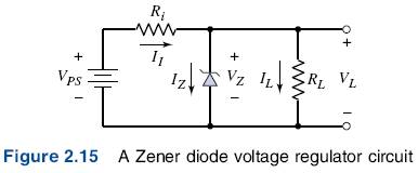
We first determine the proper input resistance Ri. This resistance limits the current through the Zener diode and drops the excess voltage between VPS and VZ.
![]()
which assumes that the Zener resistance is zero for the ideal diode. Solving this equation for the diode current. Iz, we get
where 1L = Vz / RL, and the variables are the input voltage source VPS and the load current 1L.
For proper operation of this circuit, the diode must remain in the breakdown region and the power dissipation in the diode must not exceed its rated value. In other words:
Inserting these two specifications into the previous equation, we obtain
![]()
and
![]()
Equating these two expressions, we then obtain
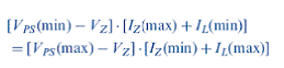
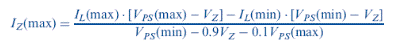
Reasonably, we can assume that we know the range of input voltage, the range of output load current, and the Zener voltage. The previous equation then contains two unknowns Iz(min) and Iz(max). Further, as a minimum requirement, we can set the minimum Zener current to be one-tenth the maximum Zener current, or IZ(min) =0.1 IZ(max). We can then solve for IZ(max), using the previous equation, as follows:
Use the maximum current obtained from the above equation, we can determine the maximum required power rating of the Zener diode. Then we can determine the required value of the input resistance using one of the previous equations.
2.2.2 Zener Resistance and Percent Regulation
In the ideal Zener diode, the Zener resistance is zero. In actual Zener diodes, however, this is not the case. The result is that the output voltage is a function of the Zener diode current or the load current. Figure 2.17 shows the equivalent circuit of the voltage regulator.
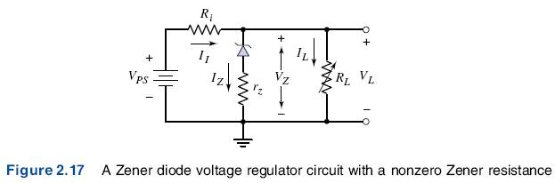
Because of the Zener resistance, the output voltage will not remain constant. We can determine the minimum and maximum values of output voltage. A figure of merit for a voltage regulator is called the percent regulation, and is defined as

where VL(nom) is the nominal value of the output voltage.
As the percent regulation approaches zero percent, the circuit approaches that of an ideal voltage regulator.
2.3 CLIPPER AND CLAMPER CIRCUITS
In this section, we continue our discussion of non-linear circuit applications of diodes. Diodes can be used in waveshaping circuits that either limit or "clip" portions of a signal, or shift the dc voltage level. The circuits are called clippers and clampers, respectively.
2.3.1 Clippers
Clipper circuits, also called limiter circuits, are used to eliminate portions of a signal that are above or below a specified level. For example, the half-wave rectifier is a clipper circuit, since all voltages below zero are eliminated. A simple application of a clipper is to limit the voltage at the input to an electronic circuit so as to prevent breakdown of the transistors in the circuit. The circuit may be used to measure the frequency of the signal, so the amplitude is not an important part of the signal.
Figure 2.18 shows the general voltage transfer characteristics of a limiter circuit.
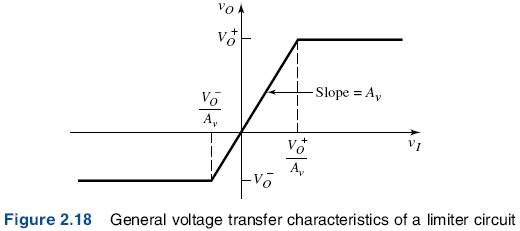
The limiter is a linear circuit if the input signal is in the range of
![]()
where Av is the slope of the transfer curve.
If Av ≤ 1, as in diode circuits, the circuit is a passive limiter. Figure 2.18 shows the general transfer curve of a double limiter, in which both the positive and negative peak values of the input signal are clipped.
Various combinations of ![]() and
and ![]() are possible. Both parameters may be positive, both negative, or one may be positive while the other negative, as indicated in the figure.
are possible. Both parameters may be positive, both negative, or one may be positive while the other negative, as indicated in the figure.
Figure 2.19(a) is a single-diode clipper circuit.
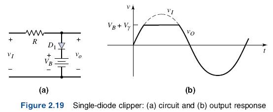
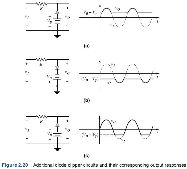
The diode Dl is off as long as vI < VB + Vγ . With D1 off, the current is zero, the voltage drop across R is zero, and the output voltage follows the input voltage. When vI > VB + Vγ , the diode turns on, the output voltage is clipped, and vo = VB + Vγ . The output signal is shown in Figure 2.19(b). Other clipping circuits can be constructed by reversing the diode, the polarity of the voltage source, or both. Figures 2.20(a). (b), and (c) show these circuits, along with the corresponding input and output signals.
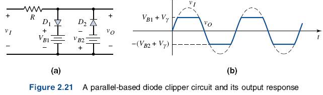
Positive and negative clipping can be performed simultaneously by using a double limiter or a parallel- based clipper, such as the circuit shown in Figure 2.21. The input and output signals are also shown in the figure. The parallel-based clipper is designed with two diodes and two voltage sources oriented in opposite directions.
2.3.2 Clampers
Clamping shifts the entire signal voltage by a dc level. In steady state, the output waveform is an exact replica of the input waveform, but the output signal is shifted by a dc value that depends on the circuit. The distinguishing feature of a clamper is that it adjusts the dc level without needing to know the exact waveform.
An example of clamping is shown in Figure 2.25(a). The sinusoidal input voltage signal is shown in Figure 2.25(b).
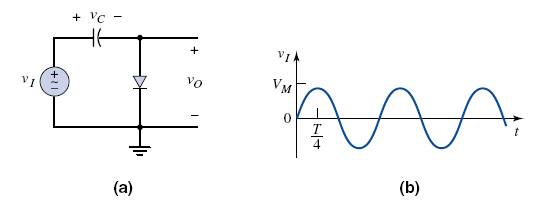
Assume that the capacitor is initially uncharged. During the first 90 degrees of the input waveform, the voltage across the capacitor follows the input, and vc = vI (assuming that rf and Vγ = 0). After vI and vc reach their peak values, vI begins to decrease and the diode becomes reverse biased. Ideally, the capacitor cannot discharge, so the voltage across the capacitor remains constant at vc = VM. By Kirchhoff's voltage law
![]()
The capacitor and output voltages are shown in Figures 2.25(c) and (d).
The output voltage is "clamped" at zero volts, that is, vo ≤ 0. In steady state, the waveshapes of the input and output signals are the same, and the output signal is shifted by a certain dc level compared to the input signal.
A clamping circuit that includes an independent voltage source VB is shown in Figure 2.26{a). In this circuit, the RLC time constant is assumed to be large, where RL is the load resistance connected to the output. If we assume, for simplicity, that rf and Vγ = 0, then the output is clamped at VB. Figure 2.26(b) shows an example of a sinusoidal input signal and the resulting output voltage signal.
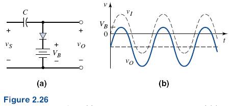
When the polarity of VB is as shown, the output is shifted in a negative voltage direction. Similarly, Figure 2.26(c) shows a square-wave input signal and the resulting output voltage signal. For the square-wave signal, we neglect the diode capacitance effects and assume the voltage can change instantaneously.
2.4 MULTIPLE-DIODE CIRCUITS
Since a diode is a nonlinear device, part of the analysis of a diode circuit involves determining whether the diode is "on" or "off." If a circuit contains more than one diode, the analysis is complicated by the various possible combinations of "on" and "off.”
In this section, we will look at several multiple-diode circuits. We will see, for example, how diode circuits can be used to perform logic functions. This section serves as an introduction to digital logic circuits that will be considered in detail in Chapters 16 and 17.
2.4.1 Example Diode Circuits
To review briefly, consider two single-diode circuits. Figure 2.30(a) shows a diode in series with a resistor. A plot of voltage transfer characteristics, v0 versus vI , shows the piecewise linear nature of this circuit (Figure 2.30{b)).
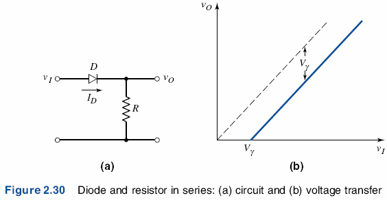
The diode does not begin to conduct until vI = Vγ . Consequently, for vI < Vγ the output voltage is zero; for vI > Vγ the output voltage is vo = vI - Vγ .
Figure 2.31(a) shows a similar diode circuit, but with the input voltage source explicitly included to show that there is a path for the diode current. The voltage transfer characteristic is shown in Figure 2.31(b).
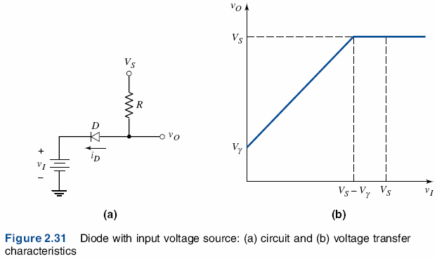
In this circuit, the diode remains conducting for vI < VS - Vγ , and the output voltage is v0 = vI + Vγ . When vI > VS - Vγ , the diode turns off and the current through the resistor is zero; therefore, the output remains constant at VS.
In multidiode circuits, each diode may be either "on" or "off." Consider the two-diode circuit in Figure 2.32. Since each diode may be either on or off, the circuit has four possible states. However, some of these states may not be feasible because of diode directions and voltage polarities.
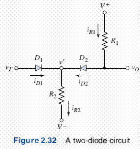
If we assume that V+ > V- and that V+ - V- > Vγ , there is a possibility that D2 can be turned on. Figure 2.33 shows the resulting plot of vo versus vI .
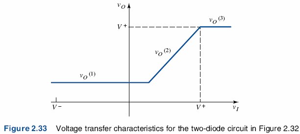
Three distinct regions are shown, corresponding to the various conducting states of Dl and D2. The fourth possible state, corresponding to both diodes being off, is not feasible in this circuit
Problem-Solving Technique: Multiple Diode Circuits
Analyzing multidiode circuits requires determining if the individual devices are "on" or "off." In many cases, the choice is not obvious, so we must initially guess the state of each device, then analyze the circuit to determine if we have a solution consistent with our initial guess. To do this, we can:
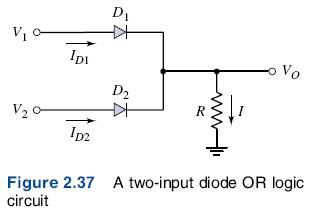
2.4.2 Diode Logic Circuits
Diodes in conjunction with other circuit elements can perform certain logic functions, such as AND and OR, but we won’t cover this except to show the circuit diagrams.

2.5 PHOTODIODE AND LED CIRCUITS
A photodiode converts an optical signal into an electrical current and a light-emitting diode (LED) transforms an electrical current into an optical signal.
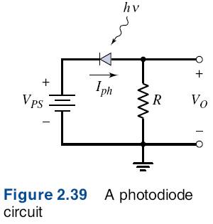
2.5.1 Photodiode Circuit
Figure 2.39 shows a typical photodiode circuit in which a reverse-bias voltage is applied to the photodiode. If the photon intensity is zero, the only current through the diode is the reverse-saturation current, which is normally very small. Photons striking the diode create excess electrons and holes in the space-charge region, where the electric field quickly separates these excess carriers and sweeps them out of the space-charge region, creating a photocurrent in the reverse-bias direction.
2.5.2 LED Circuit
A light-emitting diode (LED) is the inverse of a photodiode; that is, a current is converted into an optical signal. If the diode is forward biased, electrons and holes are injected across the space-charge region, where they become excess minority carriers. These excess minority carriers diffuse into the neutral n and p regions, where they recombine with majority carriers, and the recombination can result in the emission of a photo (with a direct band gap material such as GaAs).
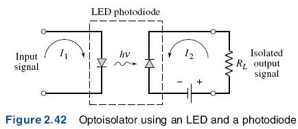
One application of LEDs and photodiodes is in opto-isolators, in which the input signal is electrically decoupled from the output (Figure 2.42). An input signal applied to the LED generates light, which is subsequently detected by the photodiode. The photodiode then converts the light back to an electrical signal. There is no electrical feedback or interaction between the output and input portions of the circuit.
2.6 SUMMARY
END Ch. 2
Source: https://chasqueweb.ufrgs.br/~hklimach/Docs/stout/Ch%202c%202006.doc
Web site to visit: https://chasqueweb.ufrgs.br
Author of the text: indicated on the source document of the above text
If you are the author of the text above and you not agree to share your knowledge for teaching, research, scholarship (for fair use as indicated in the United States copyrigh low) please send us an e-mail and we will remove your text quickly. Fair use is a limitation and exception to the exclusive right granted by copyright law to the author of a creative work. In United States copyright law, fair use is a doctrine that permits limited use of copyrighted material without acquiring permission from the rights holders. Examples of fair use include commentary, search engines, criticism, news reporting, research, teaching, library archiving and scholarship. It provides for the legal, unlicensed citation or incorporation of copyrighted material in another author's work under a four-factor balancing test. (source: http://en.wikipedia.org/wiki/Fair_use)
The information of medicine and health contained in the site are of a general nature and purpose which is purely informative and for this reason may not replace in any case, the council of a doctor or a qualified entity legally to the profession.
The texts are the property of their respective authors and we thank them for giving us the opportunity to share for free to students, teachers and users of the Web their texts will used only for illustrative educational and scientific purposes only.
All the information in our site are given for nonprofit educational purposes