
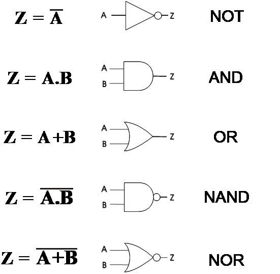
Logic gates are very useful in dealing with and processing a combination of different inputs. This switching logic can be applied to electrical switches and sensors, pneumatic valves or hydraulic systems. Switching logic uses logic gates to perform decisions. In previous work you have already seen NOT, AND and OR logic gates.
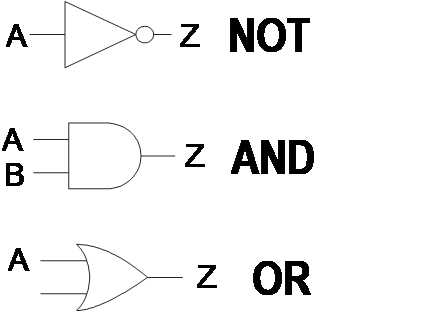
It is worth remembering that logic gates are part of digital systems and, as such, respond to either logic 1 or logic 0 signals only.
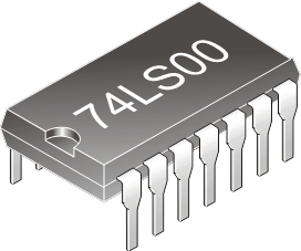
Although logic gates have electronic symbols, they are not discrete components: they are contained in integrated circuits. A typical example is the TTL7400 IC shown below. (The LS part gives more information about the chip for users.)
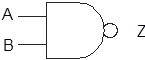
NAND logic gates are a combination of NOT and AND logic gates - see the following page.
The NAND gate is effectively an inverted AND gate. In other words, the results obtained from the output are the opposite to those of the AND gate. This gate is often referred to as ‘NOT AND’.
When drawing up the truth table for the NAND gate it can be difficult to ‘picture’ or imagine the results. The best way to do this is to pretend that it is an AND gate and then invert (reverse) the results, thus giving you the outputs for the NAND gate.
Symbol for NAND Gate
The NOR gate is effectively an inverted OR gate. In other words, the results obtained from the output are the opposite to that of the OR gate. This gate is often referred to as ‘NOT OR’.
![]()
As with the NAND gate, when drawing up the truth table for the NOR gate it can be difficult to ‘picture’ or imagine the results. The best way to do this is to pretend that it is an OR gate and then invert (reverse) the results, thus giving you the outputs for the NOR gate.
The XOR gate is a strange one off gate. It behaves like the OR gate, except that it gives a 0 when both outputs are on.
NAND gate technology can be used to build other logic gates using NAND gates only. (The same thing can be achieved using NOR gates, but NAND gate chips are more common.)
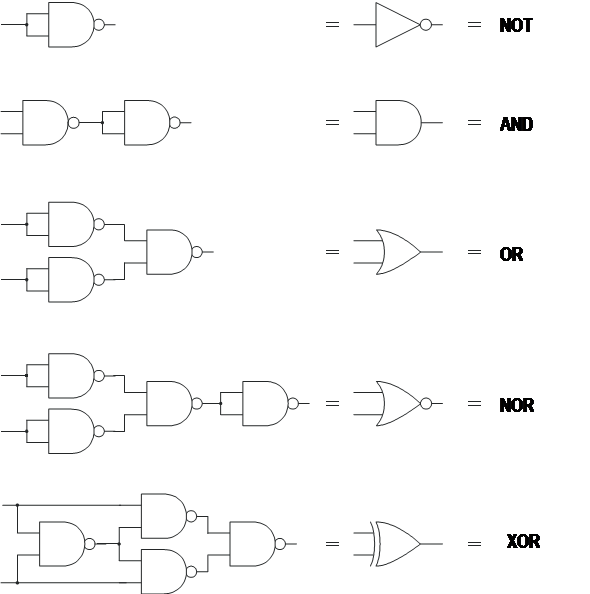
Many manufacturers use only one type of gate (normally NAND) in the manufacture of their products. This has several advantages.
The number system that we use is the decimal system; that is, we use a scale of ten. This decimal system uses 10 different digits: 0, 1, 2, 3, 4, 5, 6, 7, 8, and 9. You should have noticed that truth tables use only two digits, 0 and 1. This is called a binary system and it uses combinations of the digits 0 and 1 to form binary numbers.
The table below shows the decimal system of counting. The values of the columns (of the left-hand table) working from right to left are 1, 10, 100 and 1000. These can be written as powers of ten: 100, 101, 102, and 103. As indicated above, this type of counting is called decimal and uses a base of 10.
Decimal |
|
Binary |
|||||||
103 |
102 |
101 |
100 |
|
24 |
23 |
22 |
21 |
20 |
1000 |
100 |
10 |
1 |
|
16 |
8 |
4 |
2 |
1 |
|
|
|
0 |
|
|
|
|
|
0 |
|
|
|
1 |
|
|
|
|
|
1 |
|
|
|
2 |
|
|
|
|
1 |
0 |
|
|
|
3 |
|
|
|
|
1 |
1 |
|
|
|
4 |
|
|
|
1 |
0 |
0 |
|
|
|
5 |
|
|
|
1 |
0 |
1 |
|
|
|
6 |
|
|
|
1 |
1 |
0 |
|
|
|
7 |
|
|
|
1 |
1 |
1 |
|
|
|
8 |
|
|
1 |
0 |
0 |
0 |
|
|
|
9 |
|
|
1 |
0 |
0 |
1 |
|
|
1 |
0 |
|
|
1 |
0 |
1 |
0 |
|
|
1 |
1 |
|
|
1 |
0 |
1 |
1 |
|
|
1 |
2 |
|
|
1 |
1 |
0 |
0 |
|
|
1 |
3 |
|
|
1 |
1 |
0 |
1 |
|
|
1 |
4 |
|
|
1 |
1 |
1 |
0 |
|
|
1 |
5 |
|
|
1 |
1 |
1 |
1 |
|
|
1 |
6 |
|
1 |
0 |
0 |
0 |
0 |
As stated above, the binary system uses only two digits, 1 and 0. This system is suited to digital systems in electronics, where 1 represents ON or HIGH and 0 represents OFF or LOW.
The right-hand table shows the binary equivalents of the decimal numbers in the table on the left. The values of the columns working from right to left are 1, 2, 4, 8, and 16. These can be written in powers of 2: 20, 21, 22, 23 and 24.
The simple block diagram of the electronic system below, you will notice it has an AND gate, an OR gate and an inverter (NOT gate) in it.
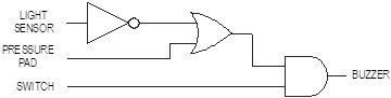
We can draw a logic diagram of this system, as shown below. There is more than one logic gate in this diagram and so it is known as a combinational logic diagram.
Drawing up a truth table for a system with more than one logic gate is not too difficult. As long as you know how each of the basic gates work, you can treat each gate on its own and then work your way through the system.
Before going ahead to look at the outputs in the truth tables, it is worth reminding ourselves of the number of combinations of inputs possible per number of actual inputs.
If there is only one input (A), then there are only two combinations (logic 0 or logic 1). So the incomplete truth table would be drawn up as below (ignoring the results in the output column, Z).
A |
Z |
0 |
|
1 |
|
If there are two inputs (A and B) they can be arranged in four different combinations:
You cannot create any other combinations. The truth table would therefore be drawn up as below (ignoring the results in the output column, Z).
A |
B |
Z |
0 |
0 |
0 |
0 |
1 |
1 |
1 |
0 |
1 |
1 |
1 |
1 |
You should notice that the input columns are arranged in binary number order.
If there are three inputs (A, B and C) they can be arranged in eight different combinations. The truth table for a 3-input system is shown below.
A |
B |
C |
Z |
0 |
0 |
0 |
|
0 |
0 |
1 |
|
0 |
1 |
0 |
|
0 |
1 |
1 |
|
1 |
0 |
0 |
|
1 |
0 |
1 |
|
1 |
1 |
0 |
|
1 |
1 |
1 |
|
The pattern in the truth tables above is clear. Starting with one input giving two combinations, you simply double the number of combinations each time an input is added.
and so on.
You will never be asked to work with a system that has more than three inputs.
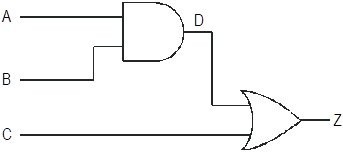
The example below shows a logic diagram that has two logic gates. There are three inputs, so this gives eight combinations in the truth table.
Draw up the results for point D.(This is the output from the AND gate, being fed by inputs A and B only.)
A |
B |
C |
D |
Z |
0 |
0 |
0 |
0 |
|
0 |
0 |
1 |
0 |
|
0 |
1 |
0 |
0 |
|
0 |
1 |
1 |
0 |
|
1 |
0 |
0 |
0 |
|
1 |
0 |
1 |
0 |
|
1 |
1 |
0 |
1 |
|
1 |
1 |
1 |
1 |
|
Draw up the results for point Z. (This is the output from the OR gate, being fed by output D and input C only.)
A |
B |
C |
D |
Z |
0 |
0 |
0 |
0 |
0 |
0 |
0 |
1 |
0 |
1 |
0 |
1 |
0 |
0 |
0 |
0 |
1 |
1 |
0 |
1 |
1 |
0 |
0 |
0 |
0 |
1 |
0 |
1 |
0 |
1 |
1 |
1 |
0 |
1 |
1 |
1 |
1 |
1 |
1 |
1 |
By following this technique, logic system problems can be solved easily.
You could use a circuit simulation program to check your results.
Each logic gate has a corresponding Boolean mathematical formula or expression. The use of these expressions saves us having to draw symbol diagrams over and over again.
The name Boolean is taken from an English mathematician, George Boole, who founded symbolic logic in the nineteenth century.
When designing systems, it is normal to design a logic diagram from a prepared truth table. This may seem difficult to start with, but if you concentrate on the combinations which give a logic 1 condition in the output column, solutions can be found easily.
The truth table below shows two inputs, A and B, and one output, Z.
A |
B |
Z |
0 |
0 |
0 |
|
1 |
0 |
|
0 |
1 |
1 |
1 |
0 |
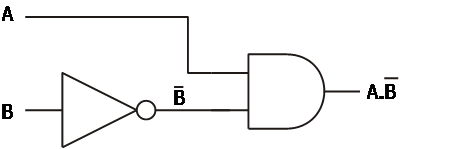
The output Z is at logic 1 in the third row down, and we can see that for this to happen A must be at logic 1 and B must be at logic 0. In other words
![]()
This means that we need a two-input AND gate, with B being fed through a NOT gate. We can write the statement in shorthand Boolean as
![]()
This means that the logic diagram is as shown below.
In this problem we have three inputs, A, B and C, with one output, Z. From the truth table we can see that there are two occasions when the output goes to logic 1.
A |
B |
C |
Z |
0 |
0 |
0 |
0 |
0 |
0 |
1 |
0 |
0 |
1 |
0 |
Z = A . B . C |
|
1 |
1 |
1 |
1 |
0 |
0 |
0 |
1 |
0 |
1 |
Z = A . B . C |
|
1 |
0 |
1 |
1 |
1 |
1 |
0 |
In other words, Z = 1 if (A is at logic 1 AND B is at logic 1 AND C is at logic 1) OR if (A is at logic 1 AND B is at logic 1 AND C is at logic 0).
This means we need a two-input OR gate being fed from two three-input AND gates as shown below.
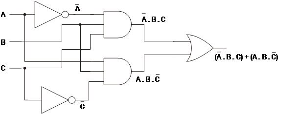
The shorthand Boolean equation for this truth table is
![]()
Perhaps the most common application of switching logic is creating a logic system to meet a given specification. Normally, by reading the specification carefully, the system designer can almost ‘see’ the required logic system.
Draw a logic diagram and a truth table for this system.
Read the specification carefully. You should notice that it has three inputs. These are:
It has one output, an alarm bell (B).
The bell should go to logic 1 if the master switch is at 1 and either the light beam goes to logic 0 or the pressure pad goes to logic 1. This can be written in Boolean as:
![]()
Note: The alarm has to be triggered when the light beam is broken and so a NOT gate is needed.
In other words, you need a two-input AND gate that is fed directly from M and also from a two-input OR gate that is fed from L (through an inverter) and P. The logic diagram is shown below.
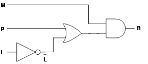
The truth table for this system is shown below. Again, all you have to do is read the specification carefully and then read across each row, one at a time, and decide whether the bell should be ringing or not. There are some short cuts. For example, in the first four rows the master switch is off; therefore the bell must be at logic 0 – even if there is a burglar in the house.
M |
L |
P |
B |
0 |
0 |
0 |
0 |
0 |
0 |
1 |
0 |
0 |
1 |
0 |
0 |
0 |
1 |
1 |
0 |
1 |
0 |
0 |
1 |
1 |
0 |
1 |
1 |
1 |
1 |
0 |
0 |
1 |
1 |
1 |
1 |
Logic gate integrated circuits (ICs)
Integrated circuits consist of plastic cases filled with electronic circuitry. There are many resistors, transistors and other components packed into the chips. There are literally thousands of ICs on the market, all designed to do different jobs – logic gates, amplifiers, timers, etc.
In this work we will be using the TTL (transistor-transistor logic) range of chips.
TTL chips require a stable 5V supply to work properly. (Great difficulties will be met if any other voltage is used.) Any unconnected pins automatically go to logic 1. In other words, if a wire connected to a pin is connected to the 0-volt rail (logic 0), it will go to logic 0. If the wire is disconnected from the 0-volt rail it will go to logic 1. However, it is good practice to connect pins to ‘high’ or ‘low’ as needed.
All TTL chips have a four-digit code number, which always starts with 74. For example, a 7400 is a quad two-input NAND chip.
Although the chip contains complex circuitry, the internal wiring can be shown as simple logic circuits with the inputs and outputs of each logic gate shown. This is called a pin-out diagram
Pin-out diagram for
7408 quad
two-input AND gate
Pin-out diagrams
ICs are impossible to use without the manufacturer’s data sheets to show what facilities are available on the chip and how the pins are to be connected. These data sheets contain pin-out diagrams. A pin-out diagram is a graphical layout of the chip and its contents.
Note: all chips have either a notch or a small dot (or both) above pin number 1 so that the user can identify all the pins without them being numbered. The dot is always at pin 1.
The description of each pin-out diagram gives details of the chip. For example, a ‘dual four-input NOR’ means the chip has two (dual) NOR gates on it, each having four inputs. A ‘quad two-input AND’ means the chip has four AND gates, each gate having two inputs.
Source: http://www.earlstonhigh.scotborders.sch.uk/learningzone/technical/Revision%20Notes/SGTS%20Revision%20Notes/5-logic.doc
Web site to visit: http://www.earlstonhigh.scotborders.sch.uk
Author of the text: indicated on the source document of the above text
If you are the author of the text above and you not agree to share your knowledge for teaching, research, scholarship (for fair use as indicated in the United States copyrigh low) please send us an e-mail and we will remove your text quickly. Fair use is a limitation and exception to the exclusive right granted by copyright law to the author of a creative work. In United States copyright law, fair use is a doctrine that permits limited use of copyrighted material without acquiring permission from the rights holders. Examples of fair use include commentary, search engines, criticism, news reporting, research, teaching, library archiving and scholarship. It provides for the legal, unlicensed citation or incorporation of copyrighted material in another author's work under a four-factor balancing test. (source: http://en.wikipedia.org/wiki/Fair_use)
The information of medicine and health contained in the site are of a general nature and purpose which is purely informative and for this reason may not replace in any case, the council of a doctor or a qualified entity legally to the profession.
The texts are the property of their respective authors and we thank them for giving us the opportunity to share for free to students, teachers and users of the Web their texts will used only for illustrative educational and scientific purposes only.
All the information in our site are given for nonprofit educational purposes