
To use a particular computer, programmers must provide commands that ultimately define a series of machine instructions. Codes can be written in a high-level language, in the intermediate symbolic code of assembly language, or directly in machine language.
An introduction to a “bare” computer system without compilers and operating systems ¾ Most of you know how to program and write algorithms, but you might not know how to manage the computer hardware. This task is usually accomplished by the Operating System (OS) which monitors the control, access and use of the resources of the machine. The OS is an “expert” in how the machine is put together, what kind of hardware is in it, what commands have to be issued to perform the correct action. It presents a uniform interface to the programmer who wants to write a program to solve a specific problem.
A bare machine does not have an OS. You, the programmer, have deal with the intricacy of the hardware yourself.
When you write a program in an high level language (C, C++, Java,…) your statements are converted into a low level code called machine code. Machine code instructions are then executed based on the actual hardware (the silicon) in the machine. A program called compiler is responsible for the conversion of the high level description of your algorithm into machine code. You normally use a text editor to write your code, run it through a compiler that produces a file containing the machine code that the OS takes and executes for you.
A bare computer does not have a compiler either.
We have such machine for you: a bare machine in a box with a power supply and a reset switch, a serial cable connected to a PC equipped with a development system. You will write code on the PC, the code is then translated to machine code and sent into the target machine where it gets executed. You will eventually debug this code.
We look at the basic structure or architecture of a typical microprocessor, the Motorola 68000 ¾ From a software developers’ point of view, the 68000 is a very elegant processor. The 6800 is the Central Processing Unit (CPU) of the overall microprocessor system you will be using.
We look at the resources available for performing computations ¾ Programmers are generally interested in programming: getting the algorithm together, writing the code, and getting it run. But you have to take a wider view of computing as you become a professional developer. For instance, you have to think at the overall performance: the speed, resources, memory and energy consumption.
1.2 Assembly Language
This is a very low-level language ¾ assembly language predates high level languages. When you write a program in C you have to specify exactly what to do. Assembly language and C share the property that the programmer orders the machine exactly what to do. The mind that you bring in programming in C is the same mind that you will bring to programming in assembly. However, the set of instructions you can force the machine to do is much more restricted in assembly than in C.
Each statement is [almost] exactly equivalent to one machine instruction ¾ A machine instruction is the lowest level operation that can be executed by the 68000 hardware. In the late 1940s it was considered that only a few number of computer machines would be needed in the world. It was seen that programming would consist of writing machine instructions. Programming was considered a very skilled operation and programmers had to write directly in machine code. Hence the introduction of assembly was a big step forward in terms ability to write and read programs.
Why learn assembly language? ¾ Programmers use high level languages to increase their personnel efficiency in developing software. When we get back down to the level of assembly language, the productivity of functionalities delivered to the end user is very low. So you may wonder why we should learn assembly.
A machine instruction is obeyed directly by machine’s hardware ¾ Because instructions are issued directly to the silicon in the machine they have to follow exactly what the machine is capable of executing.
As well as writing programs, you will find out how a computer system can interact with objects and mechanisms in the outside world - i.e. external to the computer ¾ The task of interacting with the outside world involves some part of hardware and another part of software. The hardware side is the responsibility of interfaces, often called peripherals because they are peripheral to the core computer.
Input/Output, or “IO” programming ¾ You will learn how the outside world, coming in or out of the computer, looks like in the world of computer programming and how you write programs that deal with it. This is called I/O programming.
You will be given a fast, brief, introduction to some aspects of the hardware of the computer — no knowledge of electronics necessary! ¾ Knowledge of the hardware of a computer helps you understand the origin of some of the limitations of the computer’s performances. They most typically come from the bus. The CPU is a component that executes instructions. The memory is another component that stores information. Peripheral interfaces are special-purpose devices to mediate I/O operations. They are all connected via a bus that carries information: it is a bundle of cables, like a highway where information travels. The bus has a limited speed which determines its ability to carry information. Since there is a high time cost in getting information from the memory to the processor via the bus, programmers try to keep as much information in the CPU as possible. However, the processor is a special-purpose device dedicated in executing instructions, not storing them. But what you can do is to have the processor store a tiny piece of a program, perhaps the piece of a program that is frequently used, that you can easily access. This can dramatically speed up program execution. That is called the cache. The 68000 doesn’t have one, unfortunately, but we will look at techniques to overcome this limitation.
A microprocessor is a collection of circuits packaged on a small silicon chip. It contains the basic instruction logic for a computer and the circuitry to interact with the external environment.
The 68000 is the base member of a family of microprocessors - 68010, 68020, 68030, 68040, 68060 (?)¾ The Motorola 68000 is one of a series of 16-bit microprocessors introduced in 1979. The Motorola 68000 family has been chosen to illustrate microprocessor systems because it is an excellent device for teaching purpose.
The 68000 is still produced and widely used. It continues to form the basis for a large number of commercial systems. The latest versions are embedded inside other machines like mobile phones, cars, etc. For instance, Texas Instrument uses the 68000 in its high-end graphing calculators TI89, TI92 and Voyage 200.
The 68000 is a kind of ‘CISC’ - a Complex Instruction Set Computer ¾ one of the factors influencing the architecture CISC microprocessors is the desire to help compiler writers by providing complex instruction sets. This is called closing the semantic gap (i.e. reducing the difference between high-level and low level languages). By complex instructions we mean instructions that carry out multi-step operations in a single machine-level instruction.
The course runs for all eleven weeks of the first semester and comprises three lectures and one tutorial per week, with a two-hour practical in each of the last seven weeks. Total contact time is thirty three hours of lectures, eleven hours tutorials and fourteen hours of practical sessions giving 58 hours in total.
Practicals will be marked for Continuous Assessment, which will be worth up to 20% of your course mark
The course work is a very important part of the course. The only way to learn about the computer is to use it - if you don't use it, you won't learn anything.
You are required to attend practicals and obtain a pass mark in Continuous Assessment. Failure to do so may result in the return of N/ S grades, withholding of results and/or a denial of permission to sit the Examination.
This course is intended to enable students to design and develop programs and program ‘architectures’, to test and debug programs and to analyse and modify their execution behaviour, based on a thorough familiarity with the low-level architecture of a computer. Concepts such as RISC/CISC architectures, register sets, addressing modes, data structures, subroutines, [informal] high-level to low-level language translation techniques, polling, interrupt priorities, asynchronous producer-consumer systems are introduced.
REFERENCES
Introduction to the System Bus – Signal Description
In this lecture we will describe the input and output signals of the M68000. The input and output signals can be functionally organized into the groups shown in Figure 28.1.
Note that the terms assertion and negation are used extensively in this section to avoid confusion when describing a mixture of "active-low" and "active-high" signals. The term assert or assertion is used to indicate that a signal is active or true, independently of whether that level is represented by a high or low voltage. The term negate or negation is used to indicate that a signal is inactive or false.
Learning Outcomes:
On completion of this lecture, you will be able to:

Fig. 25.1: Input and Output Signals (MC68000, MC68HC000 and MC68010)
25.1 ADDRESS BUS (A23–A1)
This 23-bit, unidirectional, three-state bus is capable of addressing 16 Mbytes of data. This bus provides the address for bus operation during all cycles except interrupt acknowledge cycles and breakpoint cycles (illegal instructions - 68010 and later).
25.2 DATA BUS (D15–D0)
This bidirectional, three-state bus is the general-purpose data path. It is 16 bits wide in the all the processors except the MC68008 which is 8 bits wide. The bus can transfer and accept data of either word or byte length.
25.3 ASYNCHRONOUS BUS CONTROL
Asynchronous data transfers are controlled by the following signals: address strobe, read/write, upper and lower data strobes, and data transfer acknowledge:
Table 25.1. Data Strobe Control of Data Bus

25.4 BUS ARBITRATION CONTROL
The bus request, bus grant, and bus grant acknowledge signals form a bus arbitration circuit to determine which device becomes the bus master device:
25.5 INTERRUPT CONTROL (IPL0, IPL1, IPL2)
These input signals indicate the encoded priority level of the device requesting an interrupt. Level seven, which cannot be masked, has the highest priority; level zero indicates that no interrupts are requested. IPL0 is the least significant bit of the encoded level, and IPL2 is the most significant bit. For each interrupt request, these signals must remain asserted until the processor signals interrupt acknowledge (FC2–FC0 and A19–A16 high) for that request to ensure that the interrupt is recognized.
25.6 SYSTEM CONTROL
The system control inputs are used to reset the processor, to halt the processor, and to signal a bus error to the processor. The outputs reset the external devices in the system and signal a processor error halt to those devices:
Either the processor retries the bus cycle or performs exception processing, as determined by interaction between the bus error signal and the halt signal.
25.7 M6800 PERIPHERAL CONTROL
These control signals are used to interface the asynchronous M68000 processors with the synchronous M6800 peripheral devices:
25.8 PROCESSOR FUNCTION CODES (FC0, FC1, FC2)
These function code outputs indicate the mode (user or supervisor) and the address space type currently being accessed, as shown in Table 28.2. The function code outputs are valid whenever AS is active.
Table 25.2. Function Code Output

25.9 CLOCK (CLK)
The clock input is a TTL-compatible signal that is internally buffered for development of the internal clocks needed by the processor. This clock signal is a constant frequency square wave that requires no stretching or shaping.
25.10 POWER SUPPLY (VCC and GND)
Power is supplied to the processor using these connections. The positive output of the power supply is connected to the VCC pins and ground is connected to the GND pins.
25.11 SIGNAL SUMMARY
Table 25.3 Signal Summary

25.13 Conclusion
The main aspects of Bus Cycles are:
REFERENCES
Introduction to the System Bus – Data Transfer Operations
After introducing the processor’s control I/O signals we now describe the signal and bus operation for some 16-bit data transfer operations including Read/Write cycle and interrupt acknowledge cycle.
Learning Outcomes:
On completion of this lecture, you will be able to:
26.1 Read Cycle
During a read cycle, the processor receives either one or two bytes of data from the memory or from a peripheral device. If the instruction specifies a word or long-word operation, the processor reads both upper and lower bytes simultaneously by asserting both upper and lower data strobes. When the instruction specifies byte operation, the processor uses the internal A0 bit to determine which byte to read and issues the appropriate data strobe:
When the data is received, the processor internally positions the byte appropriately. The read-cycle flowchart and timing diagrams are shown in Figure 29.1 and 29.2 respectively.
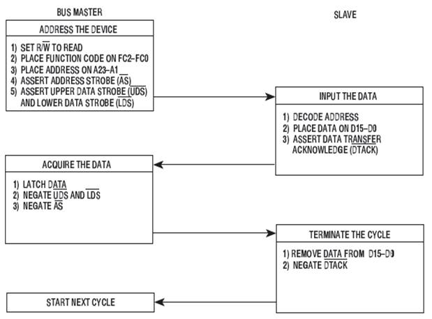
Fig. 26.1: Word Read-Cycle Flowchart
A bus cycle consists of eight states. The various signals are asserted during specific states of a read cycle, as follows:
NOTE: During an active bus cycle, VPA and BERR are sampled on every falling edge of the clock beginning with S4, and data is latched on the falling edge of S6 during a read cycle. The bus cycle terminates in S7, except when BERR is asserted in the absence of DTACK. In that case, the bus cycle terminates one clock cycle later in S9.

Fig. 26.2: Read and Write -Cycle Timing Diagrams
26.2 Write Cycle
During a write cycle, the processor sends bytes of data to the memory or peripheral device. If the instruction specifies a word operation, the processor issues both UDS and LDS and writes both bytes. When the instruction specifies a byte operation, the processor uses the internal A0 bit to determine which byte to write and issues the appropriate data strobe. When the A0 bit equals zero, UDS is asserted; when the A0 bit equals one, LDS is asserted. The word write-cycle timing diagrams and flowchart are shown in Figure 29.2 and 29.3 respectively.

Figure 26.3: Word Write-Cycle Flowchart
The descriptions of the eight states of a write cycle are as follows:
26.3 Interrupt Acknowledgement Cycle
An interrupt acknowledge cycle places the level of the interrupt being acknowledged on address bits A3–A1 and drives all other address lines high. The interrupt acknowledge cycle reads a vector number when the interrupting device places a vector number on the data bus and asserts DTACK to acknowledge the cycle. The timing diagrams for an interrupt acknowledge cycle is shown in Figure 29.4. Alternately, the interrupt acknowledge cycle can be autovectored. The interrupt acknowledge cycle is the same, except the interrupting device asserts VPA instead of DTACK. For an autovectored interrupt, the vector number used is $18 plus the interrupt level. This is generated internally by the microprocessor when VPA (or AVEC) is asserted on an interrupt acknowledge cycle. DTACK and VPA (AVEC) should never be simultaneously asserted.

Figure 26.4: Interrupt acknowledgement Cycle Timing Diagram
26.4 Conclusion
Transfer of data between devices involves the following signals: Address bus A1 through highest numbered address line, Data bus D0 through D15 and Control signals. The address and data buses are separate parallel buses used to transfer data using an asynchronous bus structure. In all cases, the bus master must deskew all signals it issues at both the start and end of a bus cycle. In addition, the bus master must deskew the acknowledge and data signals from the slave device.
What happens with an unimplemented address? i.e. the bus master attempts to read/write from/to an address that isn’t used by any slave (thus, no slave responds): we need some extra hardware, typically a simple timer, to time out if a cycle goes on too long. If the timer times out, it signals a problem by asserting BERR’.
REFERENCES:
Source: http://www.mee.tcd.ie/~assambc/3d1_l01.doc
http://www.mee.tcd.ie/~assambc/3d1_l25n.doc
http://www.mee.tcd.ie/~assambc/3d1_l26n.doc
Web site to visit: http://www.mee.tcd.ie
Author of the text: indicated on the source document of the above text
If you are the author of the text above and you not agree to share your knowledge for teaching, research, scholarship (for fair use as indicated in the United States copyrigh low) please send us an e-mail and we will remove your text quickly. Fair use is a limitation and exception to the exclusive right granted by copyright law to the author of a creative work. In United States copyright law, fair use is a doctrine that permits limited use of copyrighted material without acquiring permission from the rights holders. Examples of fair use include commentary, search engines, criticism, news reporting, research, teaching, library archiving and scholarship. It provides for the legal, unlicensed citation or incorporation of copyrighted material in another author's work under a four-factor balancing test. (source: http://en.wikipedia.org/wiki/Fair_use)
The information of medicine and health contained in the site are of a general nature and purpose which is purely informative and for this reason may not replace in any case, the council of a doctor or a qualified entity legally to the profession.
The texts are the property of their respective authors and we thank them for giving us the opportunity to share for free to students, teachers and users of the Web their texts will used only for illustrative educational and scientific purposes only.
All the information in our site are given for nonprofit educational purposes