
FIELD EFFECT TRANSISTOR
6.1 INTRODUCTION
6.2 CLASSIFICATION OF FET:
![]() There are two major categories of field effect transistors:
There are two major categories of field effect transistors:
1. Junction Field Effect Transistors
2. MOSFETs
These are further sub divided in to P- channel and N-channel devices.
MOSFETs are further classified in to two types Depletion MOSFETs and Enhancement . MOSFETs
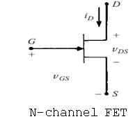
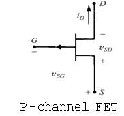
When the channel is of N-type the JFET is referred to as an N-channel JFET ,when the channel is of P-type the JFET is referred to as P-channel JFET.
The schematic symbols for the P-channel and N-channel JFETs are shown in the figure.
6.3 CONSTRUCTION AND OPERATION OF N- CHANNEL FET
If the gate is an N-type material, the channel must be a P-type material.
CONSTRUCTION OF N-CHANNEL JFET
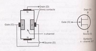
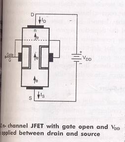
A piece of N- type material, referred to as channel has two smaller pieces of P-type material attached to its sides, forming PN junctions. The channel ends are designated as the drain and source . And the two pieces of P-type material are connected together and their terminal is called the gate. Since this channel is in the N-type bar, the FET is known as N-channel JFET.
OPERATION OF N-CHANNEL JFET:-
The overall operation of the JFET is based on varying the width of the channel to control the drain current.
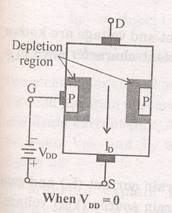
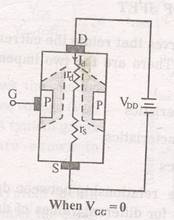
A piece of N type material referred to as the channel, has two smaller pieces of P type material attached to its sites, farming PN –Junctions. The channel’s ends are designated the drain and the source. And the two pieces of P type material are connected together and their terminal is called the gate. With the gate terminal not connected and the potential applied positive at the drain negative at the source a drain current Id flows. When the gate is biased negative with respective to the source the PN junctions are reverse biased and depletion regions are formed. The channel is more lightly doped than the P type gate blocks, so the depletion regions penetrate deeply into the channel. Since depletion region is a region depleted of charge carriers it behaves as an Insulator. The result is that the channel is narrowed. Its resistance is increased and Id is reduced. When the negative gate bias voltage is further increased, the depletion regions meet at the center and Id is cut off completely.
There are two ways to control the channel width
1 By varying the value of Vgs :-
We can vary the width of the channel and in turn vary the amount of drain current. This can be done by varying the value of Vgs. This point is illustrated in the fig below. Here we are dealing with N channel FET. So channel is of N type and gate is of P type that constitutes a PN junction. This PN junction is always reverse biased in JFET operation .The reverse bias is applied by a battery voltage Vgs connected between the gate and the source terminal i.e positive terminal of the battery is connected to the source and negative terminal to gate.
2 Varying the value of Vds holding Vgs constant :-
When both Vgs and Vds is applied:-
It is of course in principle not possible for the channel to close Completely and there by reduce the current Id to Zero for, if such indeed, could be the case the gate voltage Vgs is applied in the direction to provide additional reverse bias
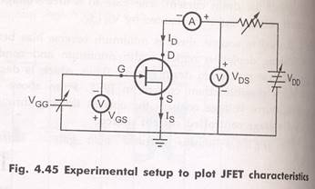
6.4 CHARACTERISTICS OF N-CHANNEL JFET :-
The family of curves that shows the relation between current and voltage are known as characteristic curves.
There are two important characteristics of a JFET.
Drain characteristics shows the relation between the drain to source voltage Vds and drain current Id. In order to explain typical drain characteristics let us consider the curve with Vgs= 0.V.

4) It is because of the fact that there is an increase in VDS .This in turn increases the reverse bias voltage across the gate source junction .As a result of this depletion region grows in size thereby reducing the effective width of the channel.
5) All the drain to source voltage corresponding to point the channel width is reduced to a minimum value and is known as pinch off.
6) The drain to source voltage at which channel pinch off occurs is called pinch off voltage(Vp).
PINCH OFF Region:-
Id =Idss [1-Vgs/Vp]2
This is known as shokley’s relation.
BREAKDOWN REGION:-
This causes
These curves shows the relationship between drain current ID and gate to source voltage VGS for different values of VDS.
Id=Idss[1-Vgs/Vgsoff]2
DIFFERENCE BETWEEN Vp AND Vgsoff –
Vp is the value of Vgs that causes the JFET to become constant current component, It is measured at Vgs =0V and has a constant drain current of Id =Idss .Where Vgsoff is the value of Vgs that reduces Id to approximately zero.
Why the gate to source junction of a JFET be always reverse biased ?
The gate to source junction of a JFET is never allowed to become forward biased because the gate material is not designed to handle any significant amount of current. If the junction is allowed to become forward biased, current is generated through the gate material. This current may destroy the component.
There is one more important characteristic of JFET reverse biasing i.e. J FET ‘s have extremely high characteristic gate input impedance. This impedance is typically in the high mega ohm range. With the advantage of extremely high input impedance it draws no current from the source. The high input impedance of the JFET has led to its extensive use in integrated circuits. The low current requirements of the component makes it perfect for use in ICs. Where thousands of transistors must be etched on to a single piece of silicon. The low current draw helps the IC to remain relatively cool, thus allowing more components to be placed in a smaller physical area.
6.5 JFET PARAMETERS
The electrical behavior of JFET may be described in terms of certain parameters. Such parameters are obtained from the characteristic curves.
A C Drain resistance(rd):
It is also called dynamic drain resistance and is the a.c.resistance between the drain and source terminal,when the JFET is operating in the pinch off or saturation region.It is given by the ratio of small change in drain to source voltage ∆Vds to the corresponding change in drain current ∆Id for a constant gate to source voltage Vgs.
Mathematically it is expressed as rd=∆Vds/ ∆Id where Vgs is held constant.
TRANCE CONDUCTANCE (gm):
It is also called forward transconductance . It is given by the ratio of small change in drain current (∆Id) to the corresponding change in gate to source voltage (∆Vds)
Mathematically the transconductance can be written as
gm=∆Id/∆Vds
AMPLIFICATION FACTOR (µ)
It is given by the ratio of small change in drain to source voltage (∆Vds) to the corresponding change in gate to source voltage (∆Vgs)for a constant drain current (Id).
Thus µ=∆Vds/∆Vgs when Id held constant
The amplification factor µ may be expressed as a product of transconductance (gm)and ac drain resistance (rd)
µ=∆Vds/∆Vgs=gm rd
6.6 THE FET SMALL SIGNAL MODEL:-
The linear small signal equivalent circuit for the FET can be obtained in a manner similar to that used to derive the corresponding model for a transistor.
We can express the drain current iD as a function f of the gate voltage and drain voltage Vds.
Id =f(Vgs,Vds)------------------(1)
The transconductance gm and drain resistance rd:-
If both gate voltage and drain voltage are varied, the change in the drain current is approximated by using taylors series considering only the first two terms in the expansion
∆id=![]() |vds=constant .∆vgs
|vds=constant .∆vgs![]() |vgs=constant∆vds
|vgs=constant∆vds
we can write ∆id=id
∆vgs=vgs
∆vds=vds
Id=gm v![]() Vds→(1)
Vds→(1)
Where gm=![]() |Vds
|Vds ![]()
![]() |Vds
|Vds
gm=![]() |Vds
|Vds
Is the mutual conductance or transconductance .It is also called as gfs or yfs common source forward conductance .
The second parameter rd is the drain resistance or output resistance is defined as
rd=![]() |Vgs
|Vgs ![]() |Vgs=
|Vgs=![]() |Vgs
|Vgs
rd=![]() |Vgs
|Vgs
The reciprocal of the rd is the drain conductance gd .It is also designated by Yos and Gos and called the common source output conductance . So the small signal equivalent circuit for FET can be drawn in two different ways.
1.small signal current –source model
2.small signal voltage-source model.
A small signal current –source model for FET in common source configuration can be drawn satisfying Eq→(1) as shown in the figure(a)
This low frequency model for FET has a Norton’s output circuit with a dependent current generator whose magnitude is proportional to the gate-to –source voltage. The proportionality factor is the transconductance ‘gm’. The output resistance is ‘rd’. The input resistance between the gate and source is infinite, since it is assumed that the reverse biased gate draws no current. For the same reason the resistance between gate and drain is assumed to be infinite.
The small signal voltage-source model is shown in the figure(b).
This can be derived by finding the Thevenin’s equivalent for the output part of fig(a) .
These small signal models for FET can be used for analyzing the three basic FET amplifier configurations:
1.common source (CS) 2.common drain (CD) or source follower
3. common gate(CG).
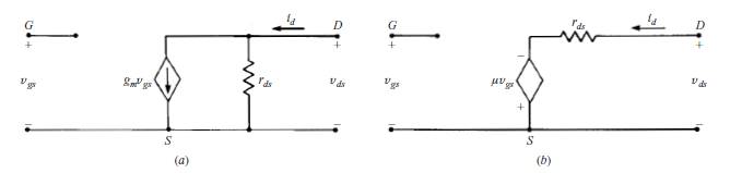 (a)Small Signal Current source model for FET (b)Small Signal voltage source model for FET
Here the input circuit is kept open because of having high input impedance and the output circuit satisfies the equation for ID
6.7 MOSFET:-
We now turn our attention to the insulated gate FET or metal oxide semi conductor FET which is having the greater commercial importance than the junction FET.
Most MOSFETS however are triodes, with the substrate internally connected to the source. The circuit symbols used by several manufacturers are indicated in the Fig below.
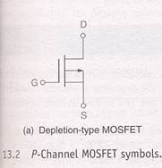
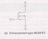
(a) Depletion type MOSFET (b) Enhancement type MOSFET
Both of them are P- channel
Here are two basic types of MOSFETS
(1) Depletion type (2) Enhancement type MOSFET.
D-MOSFETS can be operated in both the depletion mode and the enhancement mode. E MOSFETS are restricted to operate in enhancement mode. The primary difference between them is their physical construction.
The construction difference between the two is shown in the fig given below.
As we can see the D MOSFET have physical channel between the source and drain terminals(Shaded area)
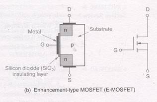
The E MOSFET on the other hand has no such channel physically. It depends on the gate voltage to form a channel between the source and the drain terminals.
Both MOSFETS have an insulating layer between the gate and the rest of the component. This insulating layer is made up of SIO2 a glass like insulating material. The gate material is made up of metal conductor .Thus going from gate to substrate, we can have metal oxide semi conductor which is where the term MOSFET comes from.
Since the gate is insulated from the rest of the component, the MOSFET is sometimes referred to as an insulated gate FET or IGFET.
The foundation of the MOSFET is called the substrate. This material is represented in the schematic symbol by the center line that is connected to the source.
In the symbol for the MOSFET, the arrow is placed on the substrate. As with JFET an arrow pointing in represents an N-channel device, while an arrow pointing out represents p-channel device.
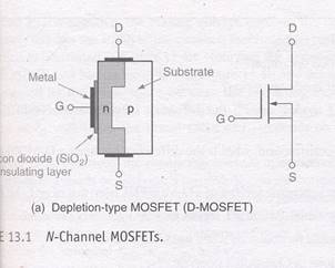
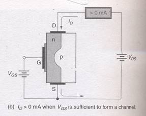
CONSTRUCTION OF AN N-CHANNEL MOSFET:-
The N- channel MOSFET consists of a lightly doped p type substance into which two heavily doped n+ regions are diffused as shown in the Fig. These n+ sections , which will act as source and drain. A thin layer of insulation silicon dioxide (SIO2) is grown over the surface of the structure, and holes are cut into oxide layer, allowing contact with the source and drain. Then the gate metal area is overlaid on the oxide, covering the entire channel region.Metal contacts are made to drain and source and the contact to the metal over the channel area is the gate terminal.The metal area of the gate, in conjunction with the insulating dielectric oxide layer and the semiconductor channel, forms a parallel plate capacitor. The insulating layer of sio2
Is the reason why this device is called the insulated gate field effect transistor. This layer results in an extremely high input resistance (10 10 to 10power 15ohms) for MOSFET.
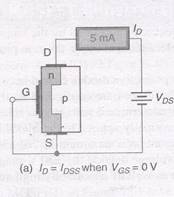
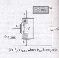
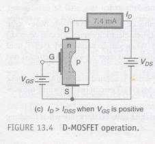
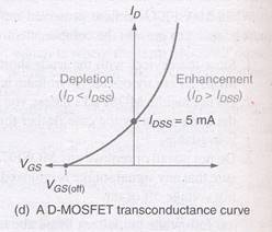
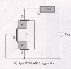
6.7.1 DEPLETION MOSFET
The basic structure of D –MOSFET is shown in the fig. An N-channel is diffused between source and drain with the device an appreciable drain current IDSS flows foe zero gate to source voltage, Vgs=0.
Depletion mode operation:-
Enhancement mode operation of the D-MOSFET:-
Characteristics of Depletion MOSFET:-
The fig. shows the drain characteristics for the N channel depletion type MOSFET
.
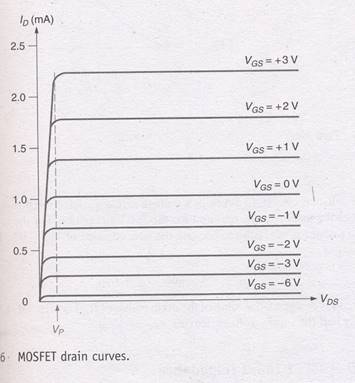
TRANSFER CHARACTERISTICS:-
The combination of 3 operating states i.e. Vgs=0V, VGs<0V, Vgs>0V is represented by the D MOSFET transconductance curve shown in Fig.
6.7.2 E-MOSFETS
The E MOSFET is capable of operating only in the enhancement mode.The gate potential must be positive w.r.t to source.
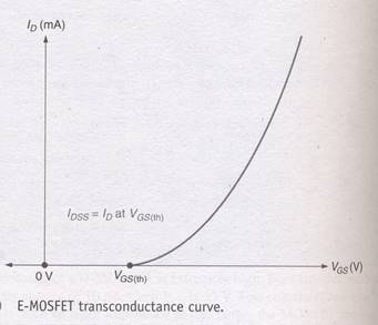
CHARACTERISTICS OF E MOSFET:-
The volt ampere drain characteristics of an N-channel enhancement mode MOSFET are given in the fig.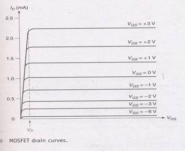
Id =K[Vgs-Vgs(Th)]2
Where K is constant for the MOSFET . found as
K=![]()
From the data specification sheets, the 2N7000 has the following ratings.
Id(on)= 75mA(minimum).
And Vgs(th)=0.8(minimum)
6.8 APPLICATION OF MOSFET
One of the primary contributions to electronics made by MOSFETs can be found in the area of digital (computer electronics). The signals in digital circuits are made up of rapidly switching dc levels. This signal is called as a rectangular wave ,made up of two dc levels (or logic levels). These logic levels are 0V and +5V.
A group of circuits with similar circuitry and operating characteristics is referred to as a logic family. All the circuits in a given logic family respond to the same logic levels, have similar speed and power-handling capabilities , and can be directly connected together. One such logic family is complementary MOS (or CMOS) logic. This logic family is made up entirely of MOSFETs.
6.9 BIASING FET:-
For the proper functioning of a linear FET amplifier, it is necessary to maintain the operating point Q stable in the central portion of the pinch off region The Q point should be independent of device parameter variations and ambient temperature variations
This can be achieved by suitably selecting the gate to source voltage VGS and drain current ID which is referred to as biasing
JFET biasing circuits are very similar to BJT biasing circuitsThe main difference between JFET circuits and BJT circuits is the operation of the active components themselves
There are mainly two types of Biasing circuits
6.9.1 SELF BIAS
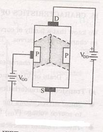
Self bias is a JFET biasing circuit that uses a source resistor to help reverse bias the JFET gate. A self bias circuit is shown in the fig. Self bias is the most common type of JFET bias. This JFET must be operated such that gate source junction is always reverse biased. This condition requires a negative VGS for an N channel JFET and a positive VGS for P channel JFET. This can be achieved using the self bias arrangement as shown in Fig. The gate resistor RG doesn’t affect the bias because it has essentially no voltage drop across it, and : the gate remains at 0V .RG is necessary only to isolate an ac signal from ground in amplifier applications. The voltage drop across resistor RS makes gate source junction reverse biased.
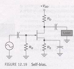
For the dc analysis coupling capacitors are open circuits.
For the N channel FET in Fig (a)
IS produces a voltage drop across RS and makes the source positive w.r.t ground. In any JFET circuit all the source current passes through the device to the drain circuit .This is due to the fact that there is no significant gate current.
We can define source current as IS = ID
(VG =0 because there is no gate current flowing in RG So VG across RG is zero)
VG =0 then VS= ISRS =ID RS
VGS = VG-VS =0-ID RS=- ID RS
DC analysis of self Bias:-
In the following DC analysis, the N channel J FET shown in the fig. is used for illustration.
For DC analysis we can replace coupling capacitors by open circuits and we can also replace the resistor RG by a short circuit equivalent.:. IG = 0.The relation between ID and VGS is given by
Id=Idss[1-![]() ]2
]2 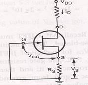
VGS for N channel JFET is =-id Rs
Substuting this value in the above equation
Id=Idss[1-![]() ]2
]2
Id=Idss[1+![]() ]2
]2
For the N-chanel FET in the above figure
Is produces a voltage drop across Rs and makes the source positive w.r.t ground in any JFET circuit all the source current passes through the device to drain circuit this is due to the fact that there is no significant gate current. Therefore we can define source current as Is=Id and Vg=0 then
Vs= Is Rs =IdRs
Vgs=Vg-Vs=0-IdRs=-IdRs
Drawing the self bias line:-
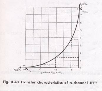
Typical transfer characteristics for a self biased JFET are shown in the fig.
The maximum drain current is 6mA and the gate source cut off voltage is -3V. This means the gate voltage has to be between 0 and -3V.
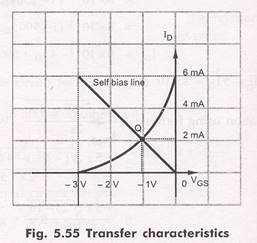
Now using the equation VGS = -IDRS and assuming RS of any suitable value we can draw the self bias line.
Let us assume RS = 500Ω
With this Rs , we can plot two points corresponding to ID = 0 and Id = IDSS
for ID = 0
VGS = -ID RS
VGS = 0X (500.Ω) = 0V
So the first point is (0 ,0)
( Id, VGS)
For ID= IDSS=6mA
VGS = (-6mA) (500 Ω) = -3V
So the 2nd Point will be (6mA,-3V)
By plotting these two points, we can draw the straight line through the points. This line will intersect the transconductance curve and it is known as self bias line.The intersection point gives the operating point of the self bias JFET for the circuit.
At Q point , the ID is slightly > than 2mA and VGS is slightly > -1V. The Q point for the self bias JFET depends on the value of Rs.If Rs is large, Q point far down on the transconductance curve ,ID is small, when Rs is small Q point is far up on the curve , ID is large.
6.9.2 VOLTAGE DIVIDER BIAS:-
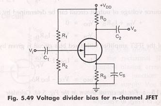
The fig. shows N channel JFET with voltage divider bias. The voltage at the source of JFET must be more positive than the voltage at the gate in order to keep the gate to source junction reverse biased. The source voltage is
VS = IDRS
The gate voltage is set by resistors R1 and R2 as expressed by the following equation using the voltage divider formula.
Vg=![]() Vdd
Vdd
For dc analysis
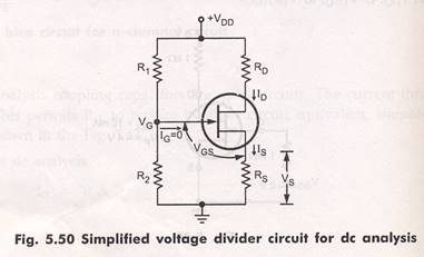
Applying KVL to the input circuit
VG-VGS-VS =0
:: VGS = VG-Vs=VG-ISRS
VGS = VG-IDRS :: IS = ID
Applying KVL to the input circuit we get
VDS+IDRD+VS-VDD =0
::VDS = VDD-IDRD-IDRS
VDS = VDD-ID ( RD +RS )
The Q point of a JFET amplifier , using the voltage divider bias is
IDQ = IDSS [1-VGS/VP]2
VDSQ = VDD-ID ( RD+RS )
COMPARISON OF MOSFET WITH JFET
Source: https://www.snscourseware.org/snsct/files/CW_595634b70671f/EDC%20unit%206%20FET.doc
Web site to visit: https://www.snscourseware.org
Author of the text: indicated on the source document of the above text
If you are the author of the text above and you not agree to share your knowledge for teaching, research, scholarship (for fair use as indicated in the United States copyrigh low) please send us an e-mail and we will remove your text quickly. Fair use is a limitation and exception to the exclusive right granted by copyright law to the author of a creative work. In United States copyright law, fair use is a doctrine that permits limited use of copyrighted material without acquiring permission from the rights holders. Examples of fair use include commentary, search engines, criticism, news reporting, research, teaching, library archiving and scholarship. It provides for the legal, unlicensed citation or incorporation of copyrighted material in another author's work under a four-factor balancing test. (source: http://en.wikipedia.org/wiki/Fair_use)
The information of medicine and health contained in the site are of a general nature and purpose which is purely informative and for this reason may not replace in any case, the council of a doctor or a qualified entity legally to the profession.
The texts are the property of their respective authors and we thank them for giving us the opportunity to share for free to students, teachers and users of the Web their texts will used only for illustrative educational and scientific purposes only.
All the information in our site are given for nonprofit educational purposes