
Problem-Solving Technique: MOSFET DC Analysis
Analyzing the dc response of a MOSFET circuit requires knowing the bias condition (saturation or non-saturation) of the transistor. In some cases, the bias condition may not be obvious, which means that we have to guess the bias condition, then analyze the circuit to determine itf we have a solution consistent with our initial guess. To do this, we can:
1. Assume that the transistor is biased in the saturation region, in which case VGS > VTN, ID > 0 and
VDS ≥ VDS(sat).
2. Analyze the circuit using the saturation current-voltage relations.
3. Evaluate the resulting bias condition of the transistor. If the assumed parameter values in step 1 are valid, then the initial assumption is correct. If VGS < VTN, then the transistor is probably cutoff, and if
VDS < VDS(sat), the transistor is likely biased in the non-saturation region.
4. If the initial assumption is proved incorrect, then a new assumption must be made and the circuit reanalyzed. Step 3 must then be repeated.
5.2.3 Common MOSFET Configurations: DC Analysis
There are various other MOSFE-T circuit configurations, in addition to the basic common-source circuit. Several examples are discussed in this section.
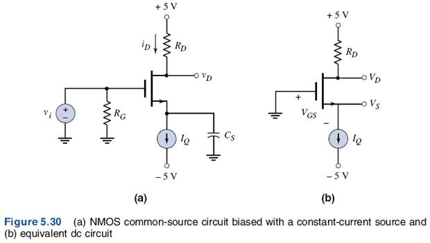
In bipolar circuits, we observed that the Q-point tended to be stabilized when an emitter resistor was included in the circuit. In a similar way, the Q-point of MOSFET circuits will tend to be stabilized against variations in transistor parameters by including a source resistor. The transistor conduction parameter may vary from one device to another because of fabrication tolerances in channel length, channel width, oxide thickness, or carrier mobility. The threshold voltage may also vary from one device to another. Variations in these device parameters will change the Q-point in a given circuit, but the change can be lessened by including a source resistor. Further, in many MOSFET circuits today, the source resistor is replaced by a constant-current source, which biases the transistor with a constant current that is independent of the transistor parameters, thereby stabilizing the Q-point.
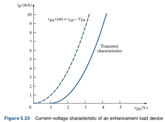
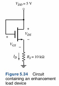
An enhancement-mode MOSFETconnected in a configuration as shown in Figure 5.32 can be used as a nonlinear resistor. A transistor with this connection is called an enhancement load device. Since the transistor is an enhancement mode device, VTn > 0. Also for this circuit, VDS = VGS > VDS(sat) = VGS - VTn which means that the transistor is always biased in the saturation region. The general I-V characteristics for such a device can then be written as
![]()
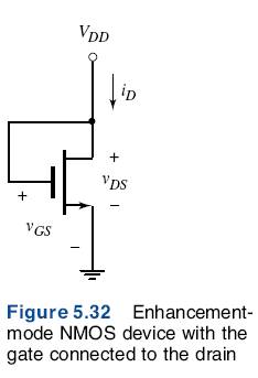
Figure 5.33 shows a plot of Equation (5.19) for the case when Kn = 1 mA / V2 and VTn = 1 V.
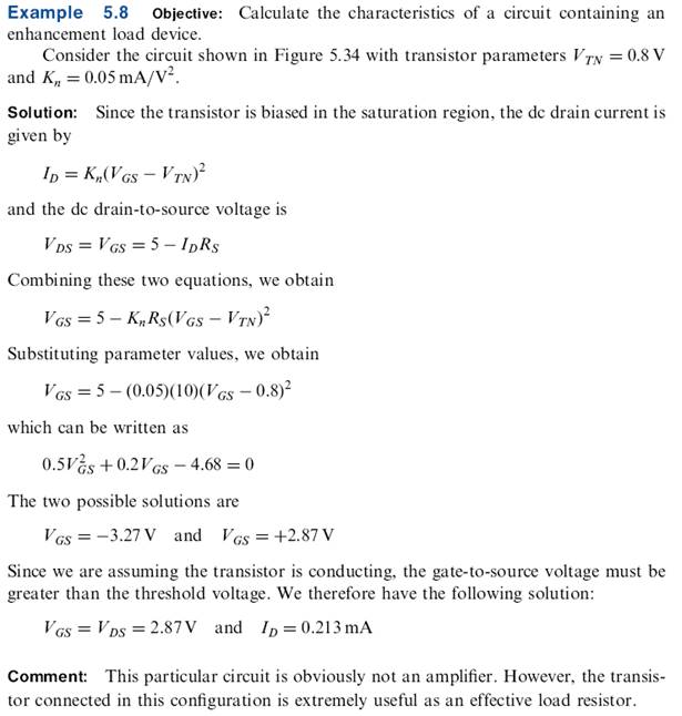
If an enhancement load device is connected in a circuit with another MOSFET in the configuration in Figure 5.35, the circuit can be used as an amplifier or as an inverter in a digital logic circuit.
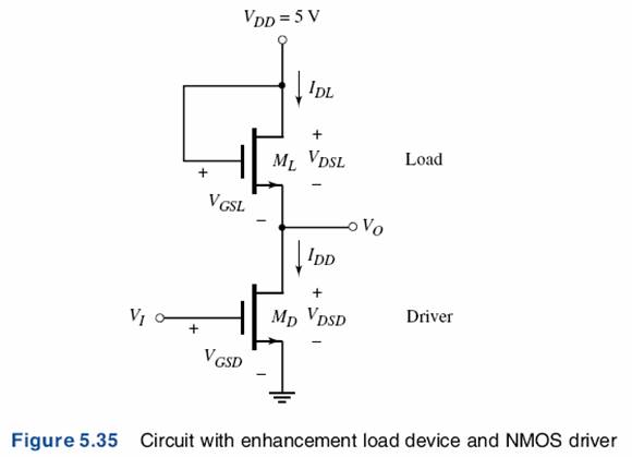
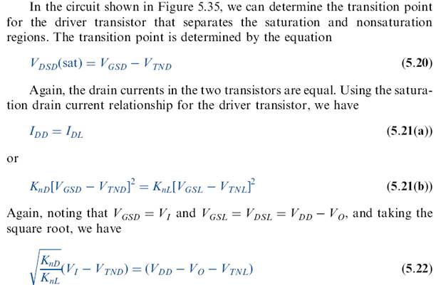
The load device, ML, is always biased in the saturation region, and the transistor MD, called the driver transistor, can be biased in either the saturation or non-saturation region, depending on the value of the input voltage. The next example addresses the dc analysis of this circuit for dc input voltages to the gate of MD.
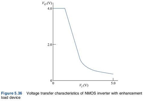
Computer Simulation: The voltage transfer characteristic of the MM OS inverter circuit with the enhancement load shown in Figure 5.35 was obtained by a PSpice analysis. These results are shown in Figure 5.36. For an input voltage less than 1 V the driver is cut off and the output voltage is VDD – VTnL =
5 – 1 = 4 V. As the input voltage decreases, the output voltage increases, charging and discharging capacitances in the transistors. When the current goes to zero at VI = 1 V and VO = 4 V, the capacitances cease charging and discharging so the output voltage cannot get to the full VDD = 5 V value.
When the input voltage is just greater than 1 V, both transistors are biased in the saturation region as the previous analysis for VI = 1.5 V showed. The output voltage is a linear function of the input voltage.
For an input voltage greater than approximately 2.25 V, the driver transistor is biased in the non-saturation region and the output voltage is a nonlinear function of the input voltage.

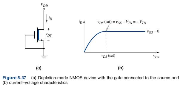
Up to this point, we have only considered the n-channel enhancement-mode MOSFET as a load device. An n-channel depletion-mode MOSFET can also be used. Consider the depletion-mode MOSFET with the gate and source connected together shown in Figure 5.37(a). The current-voltage characteristics are shown in Figure 5.37(b). The transistor may be biased in either the saturation or non-saturation regions. The transition point is also shown on the plot. The threshold voltage of the n-channel depletion-mode MOSFET is negative so that VDS(sat) is positive.
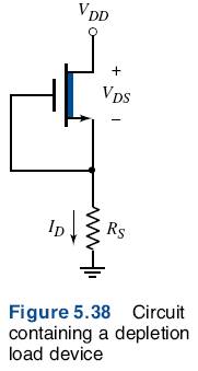
Consider the circuit shown in Figure 5.38 in which the transistor is being used as a depletion load device. It may be biased in the saturation or non-saturation region, depending on the values of the transistor parameters and VDD and RS.
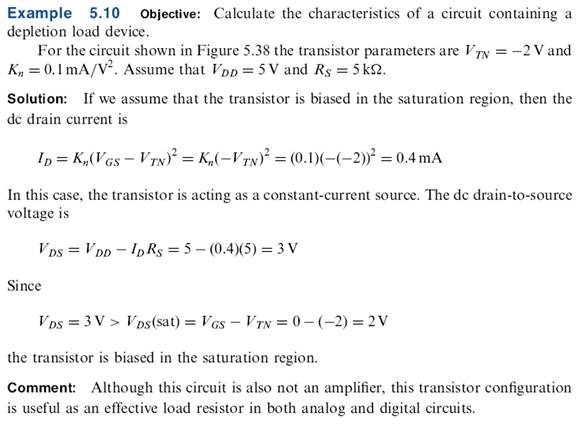
.
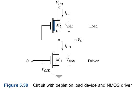
A depletion load device can be used in conjunction with another MOSFET, as shown in Figure 5.39, to create a circuit that can be used as an amplifier or as an inverter in a digital logic circuit. Both the load device ML and driver transistor MD may be biased in either the saturation or non-saturation region, depending on the value of the input voltage. We will perform the dc analysis of this circuit for a particular dc input voltage to the gate of the driver transistor.
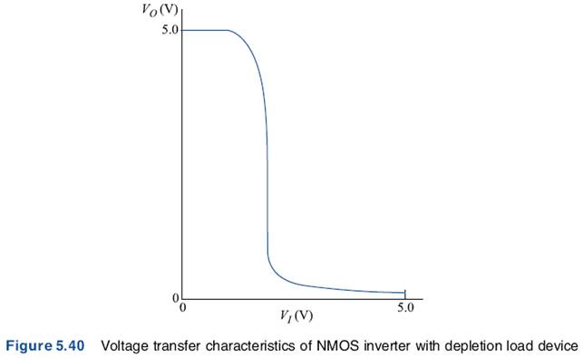
Computer Simulation: The voltage transfer characteristics of the NMOS inverter circuit with depletion load in Figure 5.39 were obtained using a PSpice analysis. These results are shown in Figure 5.40. For an input voltage less than 1 V, the driver is cut off and the output voltage is 5 V.
When the input voltage is just greater than I V, the driver transistor is biased in the saturation region and the load device in the non-saturation region. When the input voltage is approximately 1 .9V, both transistors are biased in the saturation region. If the channel length modulation parameter λ is assumed to be zero as in this example there is no change in the input voltage during this transition region. As the input voltage becomes larger than 1.9 V, the driver is biased in the non-saturation region and the load in the saturation region.
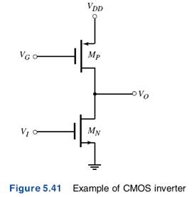
A p-channel enhancement-mode transistor can also be used as a load device to form a CMOS inverter. The term complementary implies that both n-channel and p-channel transistors are used in the same circuit. Figure 5.41 shows an example of a CMOS inverter.
5.2.4 Constant-Current Source Biasing
As was shown in Figure 5.30, a MOSFET can be biased by using a constant-current source IQ. The advantage of this circuit is that the drain current is independent of the transistor parameters.
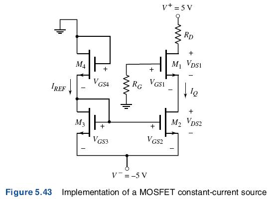
The constant-current source can be implemented by using MOSFETs as shown in Figure 5.43. The transistors M2, M3 and M4 form the current source. Transistors M3 and M4 are each connected in a diode-type configuration, and they establish a reference current. We noted in the last section that this diode-type connection implies the transistor is always biased in the saturation region. We will discuss this circuit in more detail next semester.
5.3 BASIC MOSFET APPLICATIONS: SWITCH, DIGITAL LOGIC GATE, AND AMPLIFIER
MOSFETs may be used to switch currents, voltages, and power; perform digital logic functions: and amplify small time-varying signals. In this suction, we will examine the switching properties of an NMOS transistor, analyze a simple NMOS transistor digital logic circuit, and discuss how the MOSFET can be used to amplify small signals.
5.3.1 NMOS Inverter
The MOSFET can be used as a switch in a wide variety of electronic applications. The transistor switch provides an advantage over mechanical switches in both speed and reliability. The transistor switch considered in this section is also called an inverter.
Figure 5.44 shows the n-channel enhancement-mode MOSFET inverter circuit.
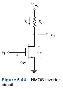
If VI < VTn the transistor is in cutoff and iD = 0 then there is no voltage drop across RD and the output voltage is VDD. Also, since iD = 0, no power is dissipated in the transistor.
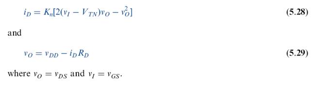
VI > VTn, the transistor is on and initially is biased in the saturation region. As the input voltage increases, the drain-to-source voltage decreases, and the transistor eventually becomes biased in the non-saturation region. When VI VDD, the transistor is biased in the non-saturation region, the output voltage reaches a minimum value, and the drain current reaches a maximum value. The current and voltage are given by
5.3.2 Digital Logic Gate
For the transistor inverter circuit in Figure 5.44, when the input is low and approximately zero volts, the transistor is cut off, and the output is high and equal to VDD. When the input is high and equal to VDD, the transistor is biased in the non-saturation region and the output reaches a low value. Since the input voltages will be either high or low, we can analyze the circuit in terms of dc parameters.
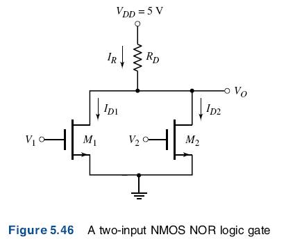
Now consider the case when a second transistor is connected in parallel, as shown in Figure 5.46. If the two inputs are zero, both M1 and M2 are cut off, and VO = 5 V. When V1 = 5 V and V2 = 0, the M1 turns on and M2 is still off. M1 is biased in the non-saturation region, and VO reaches a low value. The rest of the logic is shown in Table 5.2 below.
5.3.3 MOSFET Small-Signal Amplifier
The MOSFET, in conjunction with other circuit elements, can amplify small time-varying signals. Figure 5.47(a) shows the MOSFET small-signal amplifier, which is a common-source circuit in which a time-varying signal is coupled to the gate through a coupling capacitor. Figure 5.47(b) shows the transistor characteristics and the load line. The load line is determined for vi = 0.
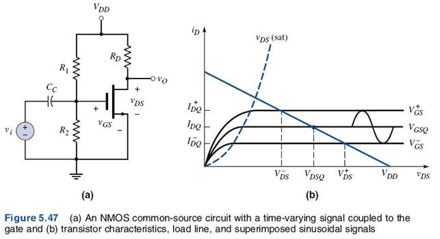
We can establish a particular Q-point on the load line by designing the ratio of the bias resistors R1 and R2. If we assume that vi = Vi sin ωt, the gate-to-source voltage will have it sinusoidal signal superimposed on the dc quiescent value. As the gate-to-source voltage changes over time, the Q-point will move up and down the line, as indicated in the figure.
Moving up and down the load line translates into a sinusoidal variation in the drain current and in the drain-to-source voltage. The variation in output voltage can be larger than the input signal voltage, which means the input signal is amplified. The actual signal gain depends on both the transistor parameters and the circuit element values.
We will skip the rest of this chapter on JFETs and MESFETs.
5.5 SUMMARY
Source: https://chasqueweb.ufrgs.br/~hklimach/Docs/stout/Ch%205b%202006.doc
Web site to visit: https://chasqueweb.ufrgs.br/
Author of the text: indicated on the source document of the above text
If you are the author of the text above and you not agree to share your knowledge for teaching, research, scholarship (for fair use as indicated in the United States copyrigh low) please send us an e-mail and we will remove your text quickly. Fair use is a limitation and exception to the exclusive right granted by copyright law to the author of a creative work. In United States copyright law, fair use is a doctrine that permits limited use of copyrighted material without acquiring permission from the rights holders. Examples of fair use include commentary, search engines, criticism, news reporting, research, teaching, library archiving and scholarship. It provides for the legal, unlicensed citation or incorporation of copyrighted material in another author's work under a four-factor balancing test. (source: http://en.wikipedia.org/wiki/Fair_use)
The information of medicine and health contained in the site are of a general nature and purpose which is purely informative and for this reason may not replace in any case, the council of a doctor or a qualified entity legally to the profession.
The texts are the property of their respective authors and we thank them for giving us the opportunity to share for free to students, teachers and users of the Web their texts will used only for illustrative educational and scientific purposes only.
All the information in our site are given for nonprofit educational purposes