1. Physical properties of thin films are different from the properties of bulk materials:
2. Substrate and its influence
3. Thickness dependence
Methods of deposition
Basic concept: melt the source and evaporate in vacuum.
Main problem: Interaction with residual gases (mean free path)
On the substrate:
K=Nd/Ng=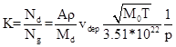
Where: A - Avogadro number, r - specific mass of the deposit [g/m3], Md - molecular mass of the deposit, vdep - speed of deposition [A/s], p – pressure [Tr].
Example: Residual gas N2, deposit Al, vdep= 1A/s
K= 1.6*10-3 @ 10-4 Tr; 1.6*10-1 @ 10-6 Tr, 1.6 *101 @ 10-8 Tr
Realistic pressures require minimum deposition speed of the order of 10 A/s
Mass evaporated in a unit time: ![]()
Two models for describing real sources:
Real source – a mixture of a number of plain and point sources
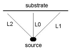
In real systems the thickness distribution does not depend only on the source characteristics but also on the source-substrate geometry.
|
L1,L2, > L0 |
Averaging by rotation – see fig 21a
Resistive (fig 21 b)
Electron beam sources
Scanning sources
Needs careful cooling
X-ray emissions
Flash sources – flash evaporation
For materials with changing composition (eg 21 e)
Substrate cooling and heating
Substrate preparation and cleaning
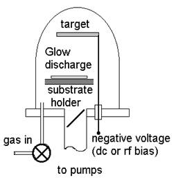
2.2. SputteringBasic concept
|
The sputtering yield: the number of neutral particles emitted per an incident ion.
See table 1.
The secondary electrons are accelerated away from the negative target with the energy of the target potential. They help to maintain the discharge. Many get thermalized but still many reach the substrate with the full energy.
The basics of SIMS(secondary ion mass spectroscopy). Most of the SIMS data deals with positive ions. In sputtering, it is highly improbable that positive ions would escape the negative target field. The negative ions result from sputtering of anionic species of compounds and high electron affinity constituents of alloys. Negative ions are accelerated away from the target toward the substrate. Due to interactions in the gas plasma arrive to the substrate as highly energetic neutrals.
No negative ions while sputtering pure metals.
The basic of ISS (ion scattering spectroscopy). One more source of substrate bombardment. These medium energy particles may be neutralized.
Leave the surface as negative ions – problems with porous targets.
While sputtering a multi-component target the composition of the surface changes due to a difference in the yield for various components. In the steady state the altered layer of a different composition from the bulk is formed. For metals the thickness of the altered layer is ![]() , for oxides
, for oxides ![]() .
.
(see fig. on page 64)
Formation of the glow discharge under increasing power from the power supply in a form of a high impedance source-
Insert fig p.64:
In subsequent steps one observes:
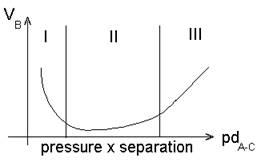
Crucial to the formation of an abnormal glow is the breakdown voltage, VB. VB depends on the mean free path of the secondary electrons and the distance dA-C between the anode and the cathode. Each secondary electron must produce 10 to 20 ions for the avalanche to occur. Paschen’s low describes the dependence of VB on the product ![]()
|
Zone I: |
Most sputtering systems operate on the border between zone I and II. This requires relatively high discharge starting voltages.
Solutions:
(See Fig. 22a)
The length of unobstructed negative glow corresponds to the range of electrons accelerated from the cathode. If the negative glow is truncated, higher voltages have to be applied to compensate for the ions that would be generated in the part blocked by the anode. In general for uniform operation the anode should be located at least 3 to 4 times the length of he cathode dark space (this distance is inversely proportional to the pressure)
ac – typically up to 50kHz where ions are mobile enough to follow the voltage and form a dc like discharge on alternating both electrodes. When f >> 50kHz we deal with rf discharge where:
How the sputtering occurs at all if ions at ![]() are relatively immobile (typical
are relatively immobile (typical ![]() =13.56 MHz). The answer: when rf bias is capacitively coupled to the electrode, pulsating negative voltage develops on the cathode – sputtering effect.
=13.56 MHz). The answer: when rf bias is capacitively coupled to the electrode, pulsating negative voltage develops on the cathode – sputtering effect.
Due to difference in mobilities of electrons and ions the I-V characteristics of a glow discharge resembles that of leaky rectifier.
(Insert fig. From page 70)
After the first cycle there is a difference in ion and electron current. Since no charge can be transferred through the capacitor the voltage on the electrode must self – bias it negatively until the net current (averaged over the cycle) is zero.
In order to sputter from the target only one couples the target via a capacitor to the generator, and the area of the capacitively coupled electrode must be small compared to the area of the dc-coupled electrode because:

![]() ,- Voltage between the glow space and the capacitively coupled electrode.
,- Voltage between the glow space and the capacitively coupled electrode. ![]() - area of the capacitively coupled electrode.
- area of the capacitively coupled electrode. ![]() ,
,![]() - voltage, area of the direct coupled electrode. To minimize the spurious sputtering from the dc coupled electrode Ad>>Ac is required. In practice the dc-coupled electrode is constituted by the system (chamber walls + baseplate), so the ratio is high.
- voltage, area of the direct coupled electrode. To minimize the spurious sputtering from the dc coupled electrode Ad>>Ac is required. In practice the dc-coupled electrode is constituted by the system (chamber walls + baseplate), so the ratio is high.
The disstribution of the potential in the system : (insert fig. on page 71)
Ions generated in a low voltage (~50V), high current (5-20A) arc discharge between a thermoionic filament and a main anode. The target is located in the main discharge and ions are extracted from it toward the target that can be powered either by dc or rf source. Triode systems are mainly used for ion etching processes requiring large amounts of ions.
Schematic of an rf sputtering equipment – insert fig p.73 (see fig. on page 73)
output power depends on the target size. It should be capable of delivering 10W/cm2 at voltage up to 5kV (this does not apply to magnetron sputtering which requires higher currents at lower voltages)
Set to one of the ISM (Industrial-Scientific-Medical) allocated frequencies. For the ISM frequencies there is no limit on the radiated power. The often used ISM frequencies are: 13.56 MHz, 27.12 MHz, and 40.68 MHz
Output impedance of rf generators is usually 50W while that of the glow discharge is much higher - matching network needed. We employ the solutions known from radio emitting generators matching to the station antenna. Matching circuitry is located close to the target assembly.
Solution for a single ended sputtering:
Insert figure p.74
For bias sputtering power splitters are needed.
Power regulating and matching is done by variable coupling:
Parameters to monitor:
In rf systems control also the matching by means of
Film specific parameters:
From a lab system to a large industrial plant.
Each application must be treated as a special case.
Work horse of the sputtering systems – Argon. Maintain constant flow and pumping to remove contamination and to operate in a pure gas. Argon purifiers: Palladium filter.
Getter sputtering
To reduce the amount of background contamination, presputter on a cooled cylinder enclosing the target, and only later open the shutter. Example: Nb, Ti, superconducting films.
Reactive sputtering:
Sputter in an active gas to obtain chemical modification of the target material.
Any material body immersed in a glow discharge acquires (when not grounded) a floating potential which is slightly negative with respect to the ground. Floating potential results from the difference in mobility of electrons and ions, and can be shown to be
![]()
Where m and Te stands for electron mass and electron temperature, respectively, M is the ion mass.
The substrate in glow discharge may be treated as floating plane Langumir probe of a characteristics:
(see fig. on page 78)
At the point Vp the probe is at the same potential as the plasma (plasma potential is
![]()
Where Ti and qi are the temperature and charge of the involved ions. The equations for Vp and Vf are drown in the approximation of no magnetic field and they can be used to evaluate Ti and Te.
N.B. If the substrate is dielectric and the holder is grounded then the substrate will be at Vs and the holder at Vs-Vf. In consequence there will be non-uniform bombardment resulting in variable thickness and composition. Good rule is “Do not ground the substrate”.
To protect deposited films or to modify their properties – biased deposition. Positive bias results in large electron current, hence heating. Negative bias enables ion implantation - e.g., deposition of TiN.
Limitations of conventional sputtering:
The magnetron sputtering principle: magnetic field is used in concert with the cathode surface to form electron traps that are so configured that E x B electron drift currents close on themselves. This method is used also in microwave generators, also named magnetron. The method can work both with dc and rf, at different configurations hollow, cylindrical, planar, or gun. (see fig 22 d,e)
Magnetron sputtering |
Classical sputtering
|
V – 800 V |
V – 3 kV |
Magnetron source is the best high rate source can be used in planar, circular or rectangular configuration (Fig. 23b).
Problems: erosion profile – max usage of the target volume up to 20% only. Solution: Patents by Sloan and Varian, the Sputter gun and the S-gun (Fig. 23 e,f)
Technical problems:
Some amazing historical remarks comments:
Primary/Direct:
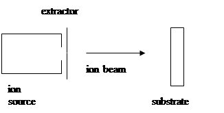
ion beam consists of the desired materials and is deposited at low energy (around 100 ev) directly onto the substrate.
Secondary
Ion sources
Penning (Fig. 23e)
The opened cathode acts also as an extractor. The spread of ion energies is 10 - 50 eV.
Kaufman (Fig. 23f)
This is an extension of the Penning concept, which includes a thermionic cathode and a proper extractor. Heated cathode allows operation at low pressures and voltages (50V). The spread of the ion energy is 1 – 10 eV. Control the emission rate by controlling the electron emission rate. Output grid – double-screen grid (~1400 holes of 0.21 mm diameter within the 10 cm dia) + accelerator grid. Density of Ar ions from a 10 cm source: 1 – 2 mA/cm2 at a beam energy of 500 – 2000 ev. Ionization efficiency ~ 75%.
Duplasmatron (Fig. 23g)
For high intensity, narrow beams. The name reflects the dual manner of constricting the plasma in an arc discharge by both electric and magnetic fields.
The filament supports 1-2A arc between the anode and the cathode (80V discharge voltage). There is “in between” electrode “Zwischen” cathode at the intermediate potential of 40V. The canal-shaped aperture in this electrode confines the discharge electrically and 0.1 – 0.3 T magnetic field between the Zwischen electrode and the anode constrains the plasma axially.
The diverging magnetic field region shapes a plasma meniscus next in the anode aperture (Fig. 22h) which becomes the emitting surface for ion extraction.
Ar ion currents above 2 mA are obtained at about 20 keV beam energy through 300 mm dia aperture with the energy spread of 10 – 50 eV.
Ion extraction
Ions in the plasma diffuse to the boundary where they can get extracted by an electric field and form a proper beam. The rate of extraction:
Child’s low of space charge limited current flow (as in a vacuum diode valve). For planer geometry – two planes at a distance d and voltage V
![]()
This is the upper limit for any particle source. The determining factors are the voltage and the electrode spacing.
For non-planar geometries the proportionality constant changes. It can be determined from the j/V3/2 ratio.
Typically one has the extraction electrode at the ground potential and the entire source at high V.
The plasma meniscus adjusts itself to satisfy the Child’s low at the local electric field. Fig. 23i shows normal extraction conditions and 23j shows excessive ion production resulting in the loss of the beam collimation.
System requirements:
Secondary ion deposition equipment
Veeco system with the 8 cm Kaufmen source, fig. 24a.
Beam diameter 7 cm, target dia. 13 cm, ion energy 200:2000 eV, beam current 30 mA.
Position 1: target presputter
Position 2: substrate precleaning
Position 3: deposition
Duplasmatron source with Einzel lens - General Louex Corp. USA. Fig. 24b:
20 keV Ar ions in 4 mm beam enables operation from very small targets, down to mg amounts of the sputtered material.
Reactive ion beam sputtering
possible configurations (insert fig. on page 87)
Primary ion beam deposition
e.g. diamond films by means of a Penning source with carbon electrodes and Argon gas. The beam consists of C ions, C neutrals, Ar ions and neutrals. (see fig. on page 88)
Typically deposition from solutions, the most popular aqueous solutions.
Deposition by a chemical reaction
e.g. Ag films for silver mirrors:
Solution of silver salt (usually AgNO3) in one solution and a reducing agent in the second solution. Two solutions are sprayed on the surface that has been "sensitized", e.g. by dipping in a solution of SnCl2 acidified with HCl.
Most common deposits Cu, Ag, Au, PbS (for coloring brass), and Ni. Deposition also on non-conduction surfaces.
Autocatalytic chemical reduction (“electroless plating”)
Deposition of a metallic coating by a controlled chemical reaction catalyzed by the metal or the alloy being deposited
( Mn+ + ne -> M0 ) only on catalytic surfaces
After the initiation of the reaction it becomes self-sustaining.
Example, Ni:
2H2PO2 + 2H2O + Ni2+ z Ni0 + H2 + 4H+ + 2HPO32-
The reaction goes as follows:
HPO2 + H2O (cat.zsurf.) HPO3- + 2H+ + H-
2H- + Ni2+ z Ni0 + H2
The efficiency may be decreased by a spurious reaction H+ + H- z H2.
Possible catalytic surface: Ni, Co, Rh, Pd, steel…Non-catalytic surface can be activated simply by touching with a catalytic agent.
Typical electroless deposits: Ni, Co, Pd, Pt, Cn, Au, Ag.
Conversion coating
Displacement deposition ("immersion plating")
Used more for recovery of the metal than for the actual plating. Known also as “cementation”.
Faraday's laws (1833):
Electrochemical equivalent weight :
![]()
For example, if Fe is being deposited from Fe2+ solution (valence change 2), e=55.85/2=27.93.
If Fe3+ would be used, then e=18.62.
N.B. an old definition of Coulomb unit: ! C is the amounts of electricity that deposits 0.001118 g of Ag from a solution.
It follows from the Faraday's law that the amounts of electricity needed to deposit 1 g electrochemical equivalent weight of any element is one Faraday
![]()
The mass of the reacting substance is
![]()
where G is mass in [g], I is current in [A], e is elect. eq. weight and t is time [s].
Important factors is electroplating
Reaction from the gas phase to form solid on the surface. There are many types of reaction:
SiH4(g) z Si(s) + 2H2(g)
SiCl4(g) + 2H2(g) z Si(s) + 4HCl(g)
SiH4(g) + O2(g) zSiO2(s) + 2H2(g)
Al2Cl6(g) + 3CO2(g) + H2(g) z Al2O3(s) + 3HCl(g) + 3CO(g)
3SiH4(g) + 4NH3(g) z Si3N4(s) + 12H2(g)
TiCl4(g) + CH4(g) zTiC(s) + 4HCl(g)
2GeI2(g) (lower temp) z Ge(s) + GeI4(g)
(CH3)3Ga(g) + AsH3(g) z GaAs(s) + 3CH4(g)
6GaAs(g) + 6HCl(g) F As4(g) + As2(g) + GaCl(g) + 3H2(s)
The reaction goes forward at high temperature and backwards at lower. Lowering the temperature in the down-stream part of the reactor initiates the deposition of GaAs(s)
Thermodynamics for calculating temperature of reaction and optimizing the chemistry. Kinetics of the reaction - all processes determine the rate.
High pressure and low pressure CVD
types of CVD reactors: examples: 24f pedestal, 24g horizontal, 24h barrel and 24j pancake
Fig 25 a – epitaxial GaAs CVD
Physical-chemical methods.
Film growth stages:
The growth kinetics, which determines the structure, texture and the state of the film surface, depends on the deposition rate and the substrate temperature.
The mechanism of condensation:
V – L – S, when the substrate is hot
V – L, when the substrate is at low temperature T<Tm/3, see 25 d, e.
Films quenched at very low temperatures have amorphous structure. This is the way to achieve metallic glasses.
Photoresists.
Negative photoresists (Fig 26a):
Resolution increases from a) to d). Chemical resistance increases from d) to a
Positive photoresists.
AZ 1350
AZ 1350 H (hard)
AZ 1350 J (electron sensitive resist)
Photoresit processing:
Fig 26 b,c,d. Projection exposure through the transparent substrate to avoid undercuts (fig. 26e)
(Carl Suss - Switzerland)
Exposition and mask aligner (Fig. 27a)
Substrate table (Fig. 27b) and table movement system (Fig. 27c)
Infrared alignment (Fig. 27d)
Laser alignment and exposition (Fig. 27e,f)
Etching process
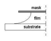
“undercut” issue |
|
Optical methods
![]()
Where N is the order, n is the refraction index of the film and d is thickness. Opaque films needs a step in the thickness down to the substrate.
Non-optical methods
![]() (Fig. 28d).
(Fig. 28d).
Source: http://physweb.bgu.ac.il/COURSES/ExperiMethods/lecture_notes/2_1_Thin_films.doc
Web site to visit: http://physweb.bgu.ac.il
Author of the text: indicated on the source document of the above text
If you are the author of the text above and you not agree to share your knowledge for teaching, research, scholarship (for fair use as indicated in the United States copyrigh low) please send us an e-mail and we will remove your text quickly. Fair use is a limitation and exception to the exclusive right granted by copyright law to the author of a creative work. In United States copyright law, fair use is a doctrine that permits limited use of copyrighted material without acquiring permission from the rights holders. Examples of fair use include commentary, search engines, criticism, news reporting, research, teaching, library archiving and scholarship. It provides for the legal, unlicensed citation or incorporation of copyrighted material in another author's work under a four-factor balancing test. (source: http://en.wikipedia.org/wiki/Fair_use)
The information of medicine and health contained in the site are of a general nature and purpose which is purely informative and for this reason may not replace in any case, the council of a doctor or a qualified entity legally to the profession.
The texts are the property of their respective authors and we thank them for giving us the opportunity to share for free to students, teachers and users of the Web their texts will used only for illustrative educational and scientific purposes only.
All the information in our site are given for nonprofit educational purposes